
Electronic Components
Global semiconductor industry to drop -22 percent in 2023! No change from May 2022!!
Global semiconductor industry is forecast to drop by -22 percent in 2023, with no change from May 2022. It remains -22 percent, as per Malcolm Penn, Founder and CEO, Future Horizons, UK, at the IFS 2023 event today.
There’s plenty to keep industry executives awake at nights. Market downturn, energy costs and inflation, interest rate rises, global recession, Russia’s war in Ukraine, China/Taiwan tension, entity list, supply chain disruption. We advice you to keep calm and carry on!
There were 2021 boom and 2022 shortages. This was no. 16! There were 15 previous upturns since the first cyclical downturn in 1961. 10 previous booms were stronger (e.g. 31.8 percent in 2010, 28 percent in 2004, and 36.8 percent in 2000). Shortages would have hit in 2018 had the market not collapsed (US-China trade war and tariffs).

The 2022 crash and 2023 downturn are also quite ‘normal.’ We had third consecutive year of positive industry growth. 1H-2021 capex spend accelerated sharply in 2H-2021 (equals capacity in 2H-2022). The industry had not had a shortage / bust since the 2000 ‘Y2K/Dot.Com’ boom. Any executive under 40 would have never lived through a classic boom-bust cycle.
When demand for goods slows down (oversupply/economic collapse), factory output falls, and expansion plans are cut. Discretionary spending slows putting pressure on services. Unsold stocks rise and selling prices come under pressure. This puts a real squeeze on the corporate cash flow and profits. If demand falls far enough, layoffs and closures are also inevitable. This causes job insecurity and demand falls even further. Even more pressure is placed on factory output as consumers spend less.
Demand eventually bottoms out, and a new equilibrium is established. Inventory has to adjust to lower production level. Factory orders fare more badly than demand. Units ordered equals units required, minus inventory burn. During a downward spiral, orders always understate the real demand.
The opposite happens, when demand for goods increases (shortages/economic boom), factory closures and layoffs abate, triggering comfort level to return. Consumers start to spend again, and factory orders start to increase. Inventory adjustment now goes positive. Job security improves substantially. Consumer spending rises even further, and further increasing demand on the factories. If demand increases enough, factories start to expand. Hiring returns, and eventually, new factories are built.
Inventory has to adjust to a higher production level. Factory orders fare better than demand. Units ordered equals units required, plus inventory build. During the upward spiral, factory orders always overstate real demand. Demand (as seen by semiconductor firms) seriously distorted — 2x during a boom, and 0.5x in a slowdown. Overshoot (both ways) is unavoidable!
Outlook 2023
The outlook for 2023 is not different this time! Only, the nuances are different, not the fundamentals. The $1-billion-dollar question — will it be -4 percent or -22 percent? Remember, the chip market always needs a strong global economy to flourish.
Unit shipments are way above the long-term average. Today, the economy is clouded in fog and uncertainty. The actual shipments were 7.8 billion/week. The real demand was 7 billion/week. Shipments are still ~10 percent over-inflated vs. trend. The gap is now steadily closing. There is supply/demand uncertainty! Correction is in progress, followed by overshoot. Then, it rebalances! We need 2-3 more quarters before balance gets fully restored.
Capex is currently running rampant! We had massive capex surge following sustained period of underinvestment. We had an eye-watering 19.8 percent of semiconductor sales in October, (but, down from September’s 21.7 percent). Q3 front-end capex surged to 17.2 percent of semiconductor sales, up from 14.6 percent in Q2. It is an all-time record 22-year high, and was unsurpassed only by Q1-2000’s 19 percent single quarter number. We need minimum of four quarters to rein in capex, when no longer needed.
ASPs rout is now in full swing. Q3-2022 ASPs were back to Q1-21 trough (past 6 quarters gain is now all gone). Expect more ASP declines going forward. As long as there is industry overcapacity, IC ASPs will drift toward costs.
Current status
The current status today is as follows. The economy has toxic mix of factors. There are supply chain disruptions, inflation, interest rate rises, public and private indebtedness, Ukraine war, China tensions, stagflation and Recession). Shipments are still ~10 percent over-inflated vs. trend. The gap is now steadily closing.
Next, unit demand is running way above long-term average. It is $7.8 billion/week vs. $7 billion trend. Shipments are still inflated, with shrinking lead times. We have slower than normal inventory burn rate, and LTA side effect?
Capacity has massive 2021-22 capex spending spree (2022 was ~flat on 2021’s $103 billion, but up 45 percent vs. 2020. We are still yet to fall! Wait for one more quarter and place in the queue, while low utilization rates are now rampant.
Finally, ASPs steep upward trajectory collapsed in June. (18 month’s supercycle ASP gain is now wiped out. Tier 2/3 Foundry ASP pricing is also under pressure. Can TSMC hold the line?
Every single warning light is still flashing red! Increase in capacity coincident with the softening market demand. There is gloomy economy outlook with high inflation / interest rate.
10 percent growth is still possible for the global semiconductor industry! But, the market’s overheating and the road ahead is stony. There is supply/demand rebalance (once the 2021 capex increases bite home). There will be slowdown in end demand. We are also seeing economic slowdown. When the bubble bursts, unit shipments plummet first, and then ASPs collapse. Don’t be surprised if the market goes negative! In May 2022, the 17th down cycle fuse was already burning. We had a collapsing chip market, coupled with a global economic downturn.
The forecast now is +4 percent (due to worsening economic outlook) or $578.302 billion vs. +6 percent in May, down from +10 percent in January 2022 (due to consumer spending squeeze). +6 percent is still just about possible, but so is +2 percent, given the magnitude of the June slowdown.
It is now anybody’s guess what December’s number actually will be! There is absolutely no insight or guidance from historical data trends. 7.4 percent quarterly decline is the best guestimate. We can confirm by early February 2023.
Driving influences
There are several key driving influences for 2023. For the economy, growth is still hampered by Covid-19-related supply chain constraints. Inflation concerns are top of the Central Bank agenda, and interest rates are yet to peak. There is an uncertain impact of reopening of China. Also, 1/3rd of the advanced economies are heading for recession (IMF, Jan. 2023).
Unit demand has excess inventory that is still not purged from the supply chain. Shipment run rates are still well above the 8 percent trend line. It may stabilize by 3Q-23. In capacity, low utilization rates are set to plague 1H-2023. Capex is yet to peak, and, it will get worse, before it gets better. 2H-2021 capex splurge is only just now on stream, just as demand ebbs away.
Finally, ASPs decline is yet to reach the bottom. The long-term ASP trend is 0 percent, as far as the last 30 years. It is hostage to Moore’s first law. IC ASPs can eventually reach ‘one dollar’, as per Moore’s second law.
It’s a hype that single-digit negative growth in 2023 is a delusion. The market would have already reached the bottom. Even trail-blazing TSMC is warning of a lousy first half of 2023. Annualized growth rates are not looking good right now. All year-on-year growth rates are now negative (IC sales is at -20 percent). Units and dollars are still falling. We are at least two quarters away from the Golden Cross.
Don’t blame memory!
Don’t just lay the blame on memory! It’s a combination of everything!! There is the tight correlation between with and without memory. We are also seeing memory first to collapse, being a commodity, and then micro, followed by logic, and finally, analog.
The 2023 forecast for the global semiconductor industry is one of no change from May 2022 — it remains -22 percent at $447.479 billion! The industry is structurally cyclical due to supply-demand mismatch. It is impossible to achieve sustainable supply and demand balance. Demand can change very rapidly (up and down), while capacity can’t! Shortages are triggered by under capacity, and the excess capacity can cause oversupply. We need to build capacity to forecast oversupply, and build to order for undersupply. We also need a new industry model. The OEMs also need to share the capex business risk.
The memo to industry executives reads: ‘Could do better’. Take some lessons from Covid-19, where you didn’t see the toilet roll manufacturers rush to build new factories during shortage! They knew high demand was a pull-forward bubble. We can work in a lot more linear manner. We need to look at where the value add is, and follow the money. Eg., services are earning $450 per cm2. End equipment is earning $35, and semiconductors $9.
It is time for the industry to rethink the supply chain. Out with the ‘Me’ vs. ‘Partnership’ business model. Out with the near-term $ vs. long-term goals and shared visions. We need to be in with balance sheet security vs. near-term gains. We need total cost of the business vs. cost saving the detail. We need strategic visionaries vs. gaming the system. Right now, IDMs are enjoying a free ride ($35-$450 vs. semiconductor firms $9).
Summary
In summary, the 17th industry down cycle is now in full flow. We are seeing collapsing demand, coupled with increased capacity, and now, a global economic downturn. There is no change from 2022 forecast.
Global semiconductor industry’s 2023 growth is still forecast at -22 percent (low, single-digit looks ‘impossible’. Worsening economic outlook will likely prolong the downturn and push recovery out. The semiconductor industry is now (finally) acknowledging that 2023 will be negative. Forward-looking data is already showing double single-digit negative.
Future Horizons advices you to keep track of the industry fundaments – don’t overthink or overhype. It’s rarely ‘different this time’, as the cycles happen! Therefore, deal with it. Prepare for the double-digit recession, as there are no soft landings. Watch out for clues, and act decisively when needed. Double down on the R&D. Invent your way out of the problem. This is the time when the design houses, IDMs, etc., do very well.
It is too early to call the outlook for 2024. We will systemically get back to low, single-digit positive growth. Magnitude and timing depends on the depth and reach of the global economic slowdown/recession. It is time to start planning for the next upturn now! You can have the first-mover advantage. The 17th industry upturn’s just around the corner!
Chips are truly the heart of everything today!
Welcome 2023! Chips are the new oil! This was proclaimed by Laith Altimime, SEMI Europe, at Semicon Europa 2022! I have been saying this for the last decade. Now, its official!
Guess what! Chips have always been truly the heart of everything! Chips are actually the heart of literally everything today that runs on electronics. That’s nearly 2/3rds of the world, or more! How could the global semiconductor industry continue to remain neglected by intelligent people, for so long, is, by itself, a huge surprise!
Semiconductors and electronic components completely rule the world! You need these two to build electronics systems. Adding photonics to these will enhance the light, speed, etc. I mentioned earlier, and repeat: Semiconductors drive everything!

For instance, imagine, if all the semiconductors of this world shut down! Imagine the colossal disaster it could bring. For instance, if TSMC were to shut down operations, 40-50 percent of the world would be brought down to its feet with grinding halt! I may be wrong in my percentage estimation, but very clear in my assessment! My job is to show the mirror to the world. People can act as they choose!
Malcolm Penn, Future Horizons, echoed the same thought. If TSMC were to go off line, whether due to the act of God (Fukushima is sitting on top of an earthquake waiting to happen) or act of political aggression (China / Hong Kong or Russia / Crimea), or, a change in business decision priorities (who gets what shipments when), the entire global economy would collapse overnight!
Dr. Nicky Lu, CEO and Founder, Etron, and Managing Board Director, Taiwan Semiconductor Industry Association (TSIA), had said TSMC’s outlook for 3.5/2.5/1.8nm production is for 2022/2024/2026, at the fifth annual heterogeneous integration symposium. Who can catch up?
I again repeat: Taiwan’s success in semiconductors has been unprecedented. I have been there several times, and seen from up close. Visit Taitronics, if you so wish! TSMC started back in 1987. It has quietly worked its way up, and today, become a super power in itself! All of this has been achieved by TSMC simply focusing on its work and delivery, rather than blowing trumpets. TSMC’s N7+ was the first commercially available extreme-UV lithographic process in the semiconductor industry. N5 iteration doubles transistor density and improves performance by an additional 15 percent. That’s something! Now, N4 will be built in USA!!
Compound semiconductors are also present everywhere! They are in RF, power, photonics, display and lighting, from components to applications. There is strong diversity of technology platforms and substrates. Applications range from photonics, such as EELs and VCSELs, to LED lighting and display, RF, and power. Perhaps, some kind of help may be taken from Taiwan.

The stance of USA and Europe towards semiconductors was surprisingly, very low, and unbecoming of them all these years. They were jolted out of their slumber by Covid-19. Soon, we had US President, Joe Biden, holding up a small chip and proclaiming the importance of semiconductors. Europe also enacted their Chips Act. Clearly, all their shares of global semiconductor market had plummeted to abysmal depths! TSMC and others have now started getting proposals to set up new fabs elsewhere. Japan has also jumped into the fray! The once electronics giant is currently reduced to a very small player in semiconductors.
With the new Chips Acts across the USA and Europe, it shows their concern about declining shares of semiconductor production, as against Asian countries. Will the Acts help them move up, perhaps, closer to Taiwan and Korea? That remains to be seen!
I still remember the ‘wicked’ smirk on that gentleman’s face — to whom I had mentioned about the growth of TSMC back in Hong Kong, 2000! I recall several talks with China executives looking to sell their products in India, in 2007-2008, when at Global Sources, Hong Kong and China!! I still remember one of the very early ISA (IESA’s original name) events, where a speaker talked about chip and system design in India. I know that several of ISA’s former leaders, have somehow dropped out of the ecosystem. USA and Europe are struggling to catch up with Asia. Can India afford to remain far behind in this race for semiconductors?
What about India?
So far, India has only taken baby steps in semiconductors. There are several plans to start manufacturing 28nm chips sometime in 2023-2024. Be aware, there are many chip lines ahead! Start counting: 28nm, 22nm, 20nm, 16nm, 14nm, 13nm, 12nm, 10nm, 7nm, 6nm, 5nm, 4nm, 3nm, 2nm, 1nm, and 3.5/2.5/1.8nm, respectively.
There were reports that Indian companies were looking to begin producing semiconductors in India within the coming years. By when? There were possibilities of partnering with existing chip manufacturers, and launching an upstream chip fabrication platform. Again, with whom? Another company stated they will begin production in about two years! People are overlooking the fact that technology moves very fast! India still does not have any R&D capability for semiconductors. It also needs to invest in advanced packaging technologies.
Is India looking at semiconductors, like it has done with IT? By the time India’s efforts in semiconductors become live, they would not be significant. Repeat, semiconductors are very different from IT. I don’t wish to say anything more, as I am not important! It will be prudent if the world, and India, can concentrate on building better chips for future!
Also, I have yet to hear of any event, or even anybody talking in India about the inclusion of women in semiconductors. People love to talk a lot about diversity, equity and inclusion (DEI). Most companies don’t have that much numbers to talk about. India, definitely not! No one, so far, has even bothered to ask the question: does India even have any ecosystem for semiconductors, let alone fabs? I happen to know some top leaders in Indian semiconductors for some time. They are welcome to contact me, if required. 😉
WSTS revised its forecast for worldwide semiconductor market in 2022 at $580 billion, up 4.4 percent, for 2022. In 2023, global semiconductor market is projected to decline by -4.1 percent to $557 billion, driven by memory segment. TSMC’s two new fabs in Arizona, USA, will manufacture over 600,000 wafers per year. TSMC is in advanced talks for setting up first potential European plant in Dresden, Germany. Intel and Samsung are also going great guns! Who else can follow them?
We are now moving slowly toward Nikola Tesla’s gospel about converting the world into a ‘huge brain’. A huge, intelligent, supercomputing brain at that! Remember, I had said: It takes pure brains to work in the global semiconductor industry!
Finally, I have really been an ‘adapter’ throughout my life! My knowledge of semiconductors is still 1 percent. I am sitting in India, and covering the global semiconductor industry. I am always hoping, sincerely, that someone from India actually reads my blog! I have always been a firm believer in leading from the front! So, it will be, and remain!!
Round-up 2022: War, chips, and back to overseas travels!
Year 2022 has been quite eventful! With the Russia-Ukraine war, alongside Covid-19, things have gone downward for the global semiconductor industry. Next year, we all hope that the industry bounces back much more stronger.
Semicon dip in 2023?
World Semiconductor Trade Statistics (WSTS) released its semiconductor market forecast generated in Nov. 2022. Following a strong growth of 26.2 percent in 2021, WSTS revised its forecast down to a single-digit growth for the worldwide semiconductor market in 2022 with a total size of $580 billion, up 4.4 percent, for 2022.
For 2023, the global semiconductor market is projected to decline by -4.1 percent to $557 billion, driven by the memory segment, according to WSTS. Will that happen? Let’s see!
Some categories are still expected to see double-digit year-over-year growth in 2022, led by analog with 20.8 percent, sensors with 16.3 percent, and logic with 14.5 percent growth. Memory is expected to turn negative in the forecast, and decline 12.6 percent year-over-year. In 2022, all geographical regions are seen to show double-digit growth except Asia Pacific. Asia Pacific is likely to decline 2 percent. Americas is expected to show growth of 17 percent, Europe 12.6 percent, and Japan 10 percent, respectively.
TrendForce, Taiwan, has said that YoY growth of NAND Flash demand bits will stay under 30 percent from 2022 to 2025 as demand slows for PC client SSDs. Recent headwinds in the global economy have caused a demand freeze in the wider consumer electronics market. Enterprise SSDs will succeed as major driver of demand bit growth in future. TSMC has also made moves in the USA, and now, is targeting Europe. More of that later!
Review 2022
In Jan. 2022, Future Horizons said that the global semiconductor industry grew 26 percent in 2021, and was likely to grow 10 percent in 2022. This was later revised down to 4 percent growth for 2022.

CEA-Leti organized a photonics workshop in Feb. 2022, where they talked about silicon photonics for AI, and integration of electronics and photonics. Dr. Nicky Lu, CEO and Founder, Etron, and Managing Board Director, Taiwan Semiconductor Industry Association (TSIA), spoke about start of tera-scale-integration era with optimized heterogeneous and monolithic integration at the fifth annual heterogeneous integration symposium, in Feb. 2021. Heterogenous integration impacts Silicon 3.0. Monolithic and heterogenous integration (MHI) has led to the Si4.0 era that is now ongoing.
March 2022 had HAXPES-Lab and what it can do for the electronics industry. There were key developments and implications of MWC 2022. DIGITALEUROPE, EU, had a webinar on how the Ukrainian IT industry was still standing against all odds, in March 2022.
ISQED 2022 was in April 2022, with Dr. Chi-foon Chan, Co-CEO, Synopsys discussing how to thrive in our changing environment. Digital Ts — threads, twins, technologies, and transformation, from Digital Twin Consortium (DTC), was another event.

May 2022 had MegaChips entering the US market for edge AI chips market. Display Week 2022 saw Ross Young discuss the smartphone and smartphone display market outlook. AR/VR market trends and technology outlook was presented by Guillaume Chansin, Director of Display Research, DSCC, at Display Week. It was in May that Future Horizons revised the semiconductor outlook for 2022 to 6 percent. Later, SEMI Arizona and Texas Chapters, USA, had a seminar on workforce shortage—meeting challenges for the semiconductor industry.
Semiconductor innovations
Global Semiconductor Alliance (GSA) had a conference on how diversity increases profitability. It looked at what managements can do to accelerate diversity. Honolulu, Hawaii, was the place for 2022 VLSI Symposium that looked at technology and circuits as critical infrastructure of future. Dr. Y. J. Mii, Senior VP of R&D, Taiwan Semiconductor Manufacturing Co. Ltd. (TSMC), presented on semiconductor innovations, from device to system.
Intel 4 CMOS with advanced FinFET transistors optimized for high-density and HPC came to the fore, and there was a workshop on cryogenic electronics for quantum computing. CHIPKIT emerged as an agile, re-usable open-source framework for test chip development. We had the OpenROAD project — open source platform for IC design innovation at VLSI Symposium 2022. Chips in Europe looked at advancing innovation in semiconductor industry, by SEMI Europe.
BloombergNEF summit in New Delhi talked about 2-4x investment that was needed to meet the net-zero targets by 2050. Semiconductor Industry Association-Semiconductor Research Corp., (SIA-SRC), USA discussed the future of semiconductor hardware. At Automatica 2022, Siemens’ showcased NX industrial electrical design to boost engineering productivity.

In July 2022, I wrote about why more women are definitely needed in semiconductors! Boreas Technology advised how piezo haptics will create their own market by introducing novel haptic apps. At Semicon West 2022, Ms. Laurie E. Locascio, Under Secretary of Commerce for Standards and Technology Director, National Institute of Standards and Technology (NIST), talked about how all parts of the US Chips Act need to be closely co-ordinated.
Andrea Lati, Director, Market Analysis, TechInsights, mentioned the semiconductor capital spending and equipment outlook for 2022. Christian Gregor Dieseldorff, Senior Principal Analyst, SEMI, discussed the trends and forecast for fab equipment spending, capacities, and new fabs.

NASA invites me!
Dr. Michael McCreary, Chief Innovation Officer, E Ink Corp., at Flex 2022, Semicon West 2022 stated how electrophoretic display was changing the look of autos, transportation, and beyond. Dr. Dawson Cagle, Program Manager, IARPA, talked about how IARPA’s smart e-pants were weaving electronics into textiles. In July, I was invited to attend NASA’s SpaceX CRS-25 launch to International Space Station. That was really something spectacular to behold!
Dr. Ms. Kate Darling, leading expert in Robot Ethics and MIT Media Lab Research Specialist, MIT Media Lab, talked about the future of human-robot interaction at Sensors Converge 2022. SIA discussed investing in innovation: blueprint for enduring American semiconductor leadership. Silicon-based quantum computing as a disruptive paradigm, was presented by Dr. Maud Vinet, Quantum Hardware Program Manager, CEA Leti, at Scaling and Lithography Tech Talks, Semicon West 2022.
Aug. 2022 saw how the EU Chips Act was necessary for accelerated digital transformation. I clarified whether people think I am very good in semiconductors? Dr. Henning Schröder, Group Leader, Fraunhofer Institute for Reliability and Micro-integration IZM, presented on glass-based quantum photonic packaging.

Agri-PV harvesting the opportunities of solar + farming started off Sept. 2022. Quantum dot imagers bridging SWIR accessibility gap was presented at SEMI MEMS & Sensors Summit 2022. Malcolm Penn, Future Horizons, revised global semiconductor growth forecast to +4 percent for 2022; with downturn likely ahead in 2023! Let’s see!
New materials required
SEMICON Taiwan 2022 Power & Opto Semiconductor Forum addressed how new materials are required to solve technology challenges, and support growth of electronics. SEMI, USA, looked into the future of computing in 2040. Center for the Study of the Presidency and Congress (CSPC), USA organized a conference on the US Chips Act and implementation. Xecs, Europe, maintained its focus on electronic components and systems.
Oct. 2022 had a session on time-sensitive networking (TSN) and future of connectivity by the Industry IoT Consortium (IIC). Satellite quantum key distribution moving to industrialization phase was discussed by the European Photonics Industry Consortium (EPIC). I also made my first overseas trip to Dubai, post the pandemic, to attend an event.
In Nov. 2022, SEMI, Northwest Chapter, USA, organized a conference on ‘The Future of More Than Moore—Chiplets, Advanced Packaging, and More’. Ms. Amy Leong, SVP, CMO, GM Emerging Growth/M&A, FormFactor Inc., presented on strategy for wafer probe in a chiplet world. Luc Van den hove, President and CEO, imec, discussed how future of scaling needs system-level thinking and STCO at IMT 2022. Japan intimated how it was gearing up to re-transform computing power and semiconductors.

Las Vegas and KA
Las Vegas, USA, welcomed me back, again, after 15 years, for an industry event. May I also mention KA, a spectacular show from Cirque de Soleil, that I witnessed. Featuring 80 artists from around the world, KÀ is a gravity-defying production featuring powerfully emotive soundtrack that enhances the innovative blend of acrobatic feats, Capoeira, puppetry, projections, and martial arts. Great experience! I also bumped into an angel or Pari, mid-air, en route to New York. 🙂
Next, there was Semicon Europa 2022 in Munich, Germany, which included ITF Beyond 5G. Among the topics discussed were compound semiconductor epitaxy core of next-gen connectivity. Chips are now the new oil, was proclaimed by Laith Altimime, President, SEMI Europe! I cannot express how happy I am to hear this! More of it later!! There were talks about building scalable and ultra-coherent quantum computers with carbon nanotubes, metaverse, future of air travel, among topics at Semicon Europa 2022. Later, there was IEEE Standards Association (SA) workshop on 5G and beyond in New Delhi.
Dec. 2022 began with an SIA seminar that looked at the growing challenge of semiconductor design leadership. Design costs are rising with every new technology node. Moore’s Law scaling has not been keeping pace. New improvements are required in design and packaging.
There are challenges to global semiconductor manufacturing. Geopolitical tensions are creating risks of disruption and shortages. Semiconductor industry is suffering from a lack of attractiveness and qualified talent. Besides, we have global warming threat and need for sustainability programs. Countries also need to create enough incentives for manufacturing investments.
Still in Dec. 2022, the 68th International Electron Devices Meeting (IEDM) 2022 was held in San Francisco, USA. IEDM celebrated its 75th birthday this year. There were five focus sessions on advanced heterogeneous integration: chiplets and system-in-packaging, quantum information and sensing, special topics in non-von Neumann computing, DNA digital data storage transistor-based DNA sequencing, and bio-computing, and implantable-device technology.

Fusion ignition achieved
US Department of Energy (DOE) and DOE’s National Nuclear Security Administration (NNSA) announced the achievement of fusion ignition at Lawrence Livermore National Laboratory (LLNL)—a major scientific breakthrough decades in the making that will pave the way for advancements in national defense and the future of clean power. On December 5, a team at LLNL’s National Ignition Facility (NIF) conducted the first controlled fusion experiment in history to reach this milestone, also known as scientific energy breakeven, meaning it produced more energy from fusion than the laser energy used to drive it.
For the first time, researchers produced more energy from fusion, than used to drive it. This promises further discovery in clean power and nuclear weapons stewardship. This historic, first-of-its kind achievement will provide unprecedented capability to support NNSA’s Stockpile Stewardship Program, and will provide invaluable insights into the prospects of clean fusion energy. It would be a game-changer for efforts to achieve President Joe Biden’s goal of a net-zero carbon economy.
TSMC leads
On December 6, TSMC announced that besides TSMC Arizona’s first fab, which is scheduled to begin production of N4 process technology in 2024, it has started construction of a second fab, scheduled to begin production of 3nm process technology in 2026. When complete, TSMC Arizona’s two fabs will manufacture over 600,000 wafers per year, with estimated end-product value of more than US$40 billion.
TSMC is also reportedly in advanced talks for setting up its first potential European plant in Dresden, Germany. The plant could begin construction by 2024. This will be probably signed sometime in 2023.
National Institute of Standards and Technology (NIST) organized a session on US CHIPS and Science Act. Ms. Gina Raimoldo, Secretary of Commerce, USA, said teams are working to ensure implementation and future impact of US Chips Act. USA is also nudging TSMC to do more in the USA.
Dec. 16, TrendForce reported that YMTC may abandon the market for 3D NAND Flash by 2024 following the US Government’s decision to place it on entity list. Well, that may be bad news for China and flash memory market.
That reminds me! I came across a post on LinkedIn, where technologies were being discussed for semiconductors by lots of big names. Ok, my name was not included! 🙂 That’s fine. Here is a list that may be looked up: nanosheets, vertical-transport nanosheet field-effect transistors (VTFETs), compound semiconductor epitaxy, quantum communications, biosensors, glass-based quantum photonic packaging, 3D hybrid electronics, piezo haptics, system-on-multichip (SoMC) architectures, tera-scale-integration, KOOL DRAM, etc. Oh, it was my BDSM moment, surely! 😉
And, that’s it, folks! 🙂 One sincerely wishes that the global semiconductor industry, and semiconductor market, are back to the top again, in 2023. Warm wishes to everyone for a very successful and vibrant 2023.
PS: Edson Arantes do Nascimento, or Pele, Brazil, and football world’s superstar, is no more. Rest in peace, ‘O Rei’, the greatest!
Xecs, Europe focuses on electronic components and systems
Xecs, Europe, organized a conference today, looking at focus areas, how to participate, and getting funded for RD&I projects. This event was organized by AENEAS that operates Xecs, PENTA and EURIPIDES² Eureka Clusters.

Xecs is a Eureka Clusters under the Eureka Clusters Program (ECP). Xecs builds on the strong legacy of Penta and Euripides², and is focused on stimulating innovative projects in the electronic components and systems (ECS) community that will address all areas of a sustainable digital transformation of the economy and society.
Xecs is a programme for the ECS community, with exploitation and growth opportunities for all the partners involved. Xecs focuses on the electronic components and systems (ECS) and their applications, and encourages innovation beyond the state-of-the-art, stimulates growth and helps create a better life for all of us.
Xecs brings together SMEs, large enterprises, research and technology organizations, and universities together into balanced, international ‘innovation ecosystems’. Xecs is designed to help you build a RD&I consortium, access funding and manage your collaborative project.
Guided by the ECS Strategic Research and Innovation Agenda prepared by experts gathered by the three Industry Associations AENEAS, EPoSS, and Inside, Xecs launches annual calls addressing the full value chain of ECS, and will benefit from the wide, dynamic innovation ecosystem stimulated by these industry associations.

Ms. Caroline Bedran, Director General, AENEAS, welcomed everyone. She said AENEAS is a non-profit association focusing on electronic components and systems, with over 580+ members. Since creation in 2008, the mission is to focus on collaborative R&D in Europe. We are actively engaged in the new Chips GU. AENEAS has been involved in several clusters for many years.
Trends in electronic components and systems
Trends in electronic components and systems was presented by Maurice Geraets, Executive Director, NXP Netherlands. Growth trends have accelerated over the last few years. There is lot of investment by EU in the Chips Act, and there is also activity in the USA. Canada, Korea, etc., are also contributing to Eureka. You can work with universities, SMEs, large corporations, etc. We address many of sustainable development goals. We are addressing climate change, ADAS, etc. We are supporting you for developing proposals and funding partnerships.
Ms. Nadja Rohrbach, Xecs Director, launched the Xecs Call 2. Xecs is a Eureka cluster supporting electronic components and systems. Over 45 countries are members of Eureka. AENEAS membership is free of charge. You can participate in trans-national RD&I co-operation and related national funding. Xecs works with idea generation, brokerage, building consortium, and getting funding.

Once you start a project, we follow that closely, to make it a real success. EFECS brokerage event will be held in Amsterdam in Nov. 22. Project outline submission deadline is 23 Feb., 23. Sept. 23 will see projects selected getting funded. There are 4-15 participants in Xecs projects. There can be minimum of two countries. Project duration is maximum 36 months. An example is the CAVIAR project, that developed and demonstrated CMOS image sensors. We currently have 23 countries supporting us. Now, we also have France, Luxembourg, UK, and Monaco, that have also supported us.

RD&I focus areas
Research, development and innovation (RD&I) focus areas was presented by Patrick Cogez, Technical Director, AENEAS. Our experts tell us where technologies will be, say 10-15 years from now. Strategic Research & Innovation Agenda (SRIA) covers the entire value chain, from materials, processes, semiconductors, etc. to smart sensors, integrated devices, etc.
The ECS-SRIA structure has the basic technology stack of typical digitalization solution heirarchical dependencies. There are transversal areas. Key apps domains are key for Europe, enabled by and driving ECS roadmap.
To use SRIA, we can give an example of a project proposal. Eg., there can be scope of mobility, along with challenges. Another can be edge intelligence, and embedded AI. An entry point is the keyword index. Eg., there can be issues such as quality, reliability, and cyber security. 2022 ECS SRIA is now available, covering the entire value chain.
National support
The last session looked at national support for funding possibilities, where representatives of public authorities presented their cases.
Ronan Bourgeois, Bpifrance, presented for France. BpiFrance is a one-stop shop for the entrepreneurs. There are two funding options available, and assistance in setting up project. In the i-Demo n2 phase, there are two options. One, minimum project size should be Euro 4 million, and maximum of six partners. Typical project duration should be from 2 to 5 years. Two, no minimum budget, and at least one French company. Project duration should be 3 years.
Kari J. Leino, Business Finland, presented for Finland. Business Finland has 50 percent funding for SMEs, 40 percent for LEs, and 70 percent for RTOs. We have continuous calls, and no fixed allocation. Normal total budget ranges from Euro 1-5 million per project. One company is enough to participate. However, if more than one RTO is involved, three Finnish companies must also participate, without BF funding.
Kasturi Narayanan, NRC-CNRC, presented for Canada. Canada is celebrating 10 years of Eureka partnership. He showed projects such as flexible phase array system, innovative systems and automated design for 5G/6G connectivity, and patient and environment aware adaptive intelligent sensor systems (pAvIs). Funding for participants is available via NRC-IRAP. Program budget is $2 million per year. We look for innovation, added value, and benefits to Canada.
Oscar Fernandez, CDTI, presented for Spain. We evaluate per company from technological and financial perspectives. We look at technology and innovation, consortium capacity, etc. We also look at commercial and exploitation plans, and socio-economic and environmental impacts. CDTI can provide credit up to 85 percent. 33 percent of credit is not reimbursable. There is long-term amortization (10-15 years).
Do you think I am very good in semiconductors?
PC, you are brilliant in semiconductors! This is a line I’ve heard several times over the years! Ok, my family does not even know this! And, why tell them? Let it be!
My standard answer: No! Why? I’ve always considered myself a student of semiconductors, and continue to do so! My knowledge of semiconductors is currently, only 1 percent! Remaining 99 percent is extremely difficult to catch up with!! Semiconductors are very complex business, and one has to be absolutely on top of the game — technically and technologically!
Yes, I know that I write very fast, and complete sessions as they finish. And, publish! That makes people swoon! I am not even bothered by all that noise!! Yes, I know a bit about technologies, but even that hasn’t bothered me to change for anyone! Never was, and never will be!! For those who have never met me, I stand 6’2″ tall, slim and wiry, or athletic, and am a born left hander, as my colleague, Madhu, used to say: Chakram leftist hai! 😉 And, I am still crazy about sports, music, astrology, Bruce Lee and martial arts, travel, etc. EEWeb decided to interview me back in 2016, when I won my first and only award from India! To every technology, and everyone: bring it on!
Components and telecom!
My career started with electronics! Naturally, that was the very first industry I dealt with. It was followed by telecom and electronic components. Association of Radio Industries and Business (ARIB), Japan, visited India and talked about PHS, or personal handyphone system. This was before GSM made an appearance. I was fascinated by an article ‘Wherever you may roam’. Then came Hong Kong, and with it, more of telecom, electronic components, and semiconductors. I also became a member of Pacific Telecom Council, Hawaii, USA, back then.
When I first visited Taiwan, I realized the depth semiconductors and electronic components have. Even today, I am surprised to see there is hardly any talk about semiconductors and components in India. How I wish that PR folks in India focus more on electronic components and semiconductors! What they have focused on, so far, is simply not relevant for me!
I recall a fellow editor from India express great surprise on learning that I was in Hong Kong! Another time, in Bangalore, I interviewed a guy who told me his interest was semiconductors. I delved deeper! The result: he wasn’t even hired!

I prepared specifications tables for telecom products at Global Sources, Hong Kong. These were: 46/49MHz phones, cellular phone antennae, transceivers, etc. In Singapore, I prepared market intelligence report for mobile accessories, covering battery chargers, battery packs, belt clips and straps, Bluetooth headsets, car kits, cell phone antennae, handsfree kits, mobile phone/pager bags and cases, mobile phone holders, mobile phone housings, mobile phone novelties, PDA accessories, radiation-protection devices, and rechargeable batteries/cells.
Now, all of these were solo efforts, as some of my colleagues at Global Sources, Hong Kong, and Reed Business, Singapore, will vouch for. Later, many others also started preparing such related tables.
When mobile Internet was first announced, there was lot of cry. It started with WAP or wireless access protocol, which was dubbed as crap! However, things changed very fast. Next came Bluetooth. Again, similar cries surfaced. However, things again changed rapidly. In Hong Kong and Singapore, my love for semiconductors, components, and optical networking further strengthened. I wrote about vertical-cavity surface emitting lasers or VCSELs. There was TD-SCDMA or time-division-synchronous code division multiple access, the 3G mobile telecom standard from China.
In India, very few had heard of TD-SCDMA, or VCSELs. There was an interesting incident though. An India company was found promoting TD-CDMA, with no S! That company’s tenure was short-lived!! Today, I find people haven’t even heard of edge-emitting lasers (EELs)! By the way, I worked for Photonics, US, and found very few takers in India. I doubt anyone has even heard of HAXPES-Lab for electronics!
Docomo’s i-mode service was making lot of noise in Japan. NTT Docomo also announced LTE. Today, we are stuck at 4G, and 5G is doing business elsewhere. 5G auctions have just been held. Now, there are talks about 5.5G and 6G. I had several interesting conversations around RoHS and WEEE standards, and their importance for electronics. RoHS stands for restriction of hazardous substances, and WEEE for waste electrical and electronic equipment.
Massachusetts Institute of Technology (MIT), USA, contacted me in 2014, when I produced an article on breast cancer. Recently, NASA invited me for the launch of SpaceX’s CRS-25 to the International Space Station. My association with global solar/PV industry also remains strong. Although, I write very little on this subject now.
Love for semiconductors
During a visit to India, Mike Splinter, then CEO, Applied Materials, talked about semiconductor sustainability and energy management. I had a conversation with Sri Peruvemba of E-Ink, regarding a revolutionary electronic ink that had paper-like high-contrast appearance, ultra-low power consumption and a thin, light form. I continue to collaborate with Sri Peruvemba and Ms. Ana Tackett for Display Week even today! 🙂 iSuppli stated that consumer and mobile MEMS supply were exploding.
My association with Dr. Walden Rhines, then CEO, Mentor Graphics, started back in 2004. It was the time for EDA industry to grow. Dr. Rhines has now moved on to Cornami and fully homomorphic encryption (FHE). Even Synopsys and Cadence Design Systems have been close to me. My association with Future Horizons, UK, and SEMI, USA, started in 2007. I have covered various semiconductor events for them. I had a similar association with Mike Cowan, independent consultant, semiconductors.

Intel and I have had a long association. It’s the same with Ericsson and Qualcomm! I first met GlobalFoundries at IEF 2010, and it continues. ARM, NXP, STMicroelectronics, Infineon, and Xilinx, have long relationships with me. My partnership with Yole Développement stands the test of time. Same goes for CEA-Leti, Imec, and Soitec, in Europe. Embedded Vision Alliance was born in 2011. However, I have dropped out of this association.
With TSMC, my association has been great! I have known them since they were small. Look at their growth now! TSMC’s CoWoS-L is the latest CoWoS process variant, and is likely to go commercial in 2023-2024. It follows CoWoS-S and CoWoS-R. We have DUV vs. EUV debate, although that’s hardly any debate! DUV or deep ultraviolet is the wavelength range in far ultraviolet chip production using 248-193nm. EUV or extreme UV is the wavelength range between 100-10nm. Now, we have PUV or plaid UV at 6.5nm. Intel may be developing that! But, can it take this beyond TSMC? Surely, TSMC will not be sitting idle!
TSMC has three innovative heterogenous integration technology (HIT) platforms, using CoWoS. These are: CoWoS, InFO_PoP (integrated fan-out package on package), and SoIC. Its 3Dblox simplifies 3DIC design flow! TSMC’s outlook for 3.5/2.5/1.8nm production is in 2022/2024/2026. Who can catch up? Intel? Difficult to say! They will have to do something really outstanding!!
Monolithic and heterogenous integration (MHI) is doing the rounds. As are monolithic DRAM or long-retention DRAM, and new, small form-factor DRAM, the RPC, or, the reduced pin-count DRAM used in AI/edge device for self-smart microsystem. Silicon 4.0 is enabling everything today.
Oh! The global semiconductor industry is officially now in downturn! Malcolm Penn, CEO, Future Horizons reported that in line with December 2021 forecast, June’s WSTS Blue Book Report confirmed the current chip boom is over! The chip market downturn has apparently started.

If you all have noticed, I haven’t even talked about any IT-related stuff! Why will there be? It’s simple! IT is way below in the technology pecking order. I’ve had really wonderful experiences working with components, electronics, and semiconductors. Why should I bother about IT? In India, I hope Thomas George, Cybermedia, continues his wonderful support of me, and semiconductors.
The correct technology order is: semiconductors, electronic components, electronics, photonics, solar/PV, telecom, Industry 4.0, etc. And, that will remain! The image shown here is based on my discussion with Ms. Iwin De’Mellow, Ms. Anindita Sarkar, and one more guy from the Archetype office at a coffee shop in Bangalore, 2018. For anyone: to gain any sort of expertise, you first need to crack the top seven rungs! It’s that simple, and difficult! 😉
Semiconductors are very difficult, as a subject. It’s like test cricket, where highly-skilled folks survive the longest. Skilled people are hard to find, and hire. India may face such problems! It is advised that you do not go for the short-term courses offered, as they are of no use. Semiconductor companies will simply not hire! You really have to take the long, hard route.
There is no trick involved here! To grow, you have to learn! You have to build relationships with the industry that you like, and maintain those over time. Just be honest with yourself, and your work! It’s quite easy! Try it! Do you still think I am very good in semiconductors?
On a personal note, I was extremely naughty as a child, and even broke my refrigerator’s lock once, just to steal and eat sweets. 😉 Continuing on that mode, here is a nice song for you! 😉
Skin head, dead head, everybody gone bad, situation aggravation, everybody, allegation
In the suite on the news, everybody, dog food, bang-bang, shock dead, everybody’s gone mad
All I wanna say is that they don’t really care about us, all I wanna say is that they don’t really care about us.
Beat me, hate me, you can never break me, will me, thrill me, you can never kill me
Jew me, sue me, everybody, do me, kick me, kike me, don’t you black or white me
All I wanna say is that they don’t really care about us, all I wanna say is that they don’t really care about us!
— Michael Jackson
PS: Friends in Indian PR industry, who have helped me in my journey: Deepa Inguva, Gayathri Mendiratta, Zibi Jamal, Kauser Jabeen, Xavier Prabhu, Pravin Rikhy, Sonali Sadanand, Shakhambari Thakur, Padmini Hegde, Tarana Utthaiya, Poornima Chikkananjaiyah, Sanjana Shetty, Seema Siddiqui, Iwin De’Mello, Puja Bhattacharji, Archit Mahajan, Anandita Sarkar, Prashansa Bharti, Debasmita Dutta, Anjali Kumari Kashyap, Sagar Desai, Gayatri Binu, Aarti Talwar, Gargi Prasad, Diksha Singh, Jatin Khattar, Kerman Kasad, etc. Thanks to everyone!
Innovative BAW filters for 5G sub-6GHz
Martin Gallezot, Business Developer, Semiconductor Technologies, CEA-Leti, presented innovative BAW filters for 5G sub-6GHz at CEA-Leti devices workshop.
Leti is very actively working on semiconductors for next-generation frontend 300GHz. This involves hybridization between silicon semiconductors and III/V semiconductors.

SAW is still no. 1, but growth is slowing. FBAR or thin-film bulk acoustic resonator is at no. 2. Main players for SAW filters are Murata, Qualcomm, Qorvo, Taiyo Yuden, Kyocera, Sunway, EpicMEMS, Wavetek, etc. BAW SMR lead players are Qorvo, Qualcomm, EpicMEMS, Unikorn, etc. FBAR players include Broadcom, Skyworks, Taiyo Yuden, etc. Piezomaterial is typically aluminum nitride. Lot of effort is paid on deposition method.
If we look at the acoustic filters for 5G NR bands, piezo-on-insulator (PoI) is the game changer. AIN is mainstream piezo material for thin-film based filters. Contenders are Sc doped AIN, LiTaO3, and LiNbO3, respectively. PoI is already in the market for SAW, and is under development for BAW. It is available upto 8″. Soitec is a leading provider of PoI. 6″ PoI is already used for SAW devices. Leti is actively working with Soitec to develop PoI.
An ongoing work at Leti is PoI-based BAW SMR and BAW FBAR on 8″ wafers. PoI-based BAW has advantages such as LNO single-crystal films on 8″ PoI wafers. We demonstrated upto 7GHz, scalable over wide range of frequencies. It leverages over 15 years of R&D at CEA-Leti. He showed a PoI-based BAW process flow.
SMR LNO results such as targeted frequency met, large Kt2 demonstrated, and good in-band performance, were published. There are challenges with TCF, heat dissipation and packaging. FBAR LNO results were nearly the same. There are remaining challenges, with packaging, new designs, and materials.
For packaging, FBAR requires Si cap with TSV. SMR can use lower cost thin-film packaging. In new designs, there are tunable SAW, tunable lamb filter, and tunable BAW. For materials, there are LiNbO3 and LiTaO3 deposition, and new electrode materials, such as AlCu, molybdenium, etc.
PHEV and BEV driving innovation in power modules
Powers module are said to hold the key in the development of power converters and inverters. Regarding the technical innovations transforming the power module packaging supply chain, Milan Rosina, Principal Analyst, Power Electronics & Batteries, Yole Développement (Yole), said that among the key innovations is the growing demand on SiC power modules toward ‘discrete-like’ power modules. These are like, one can find, for example, in the Tesla Model 3 electric car traction inverter.
Besides, high-performance packaging solutions, such as silver sintering and Si3N4 AMB ceramic substrate, offer enhanced heat thermal dissipation and improved reliability. Hence, they are increasing their technology share and attracting new players.
Faster deployment of EVs/HEVs
Let’s examine how is the faster deployment of EVs/HEVs going to help.
Rosina said: “The EV/HEV represents a unique combination of a strong technology challenge and a huge business opportunity due to big market size and strong potential for its further growth. Moreover, the money invested into development of new technologies can be rapidly paid back due to fast implementation of these innovative technologies in high volumes.
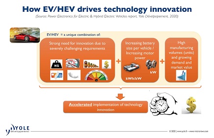
“Within the booming power module market, the trend toward stronger electrification, such as the plug-in hybrid electric vehicles (PHEV) and battery electric vehicles (BEV), especially, is increasing the potential for power electronic players. This is due to the high inverter power and needs for innovative solutions to increase inverter power density and enhance heat dissipation while maintaining the high reliability level.
Meeting challenges
Next, how are challenges, such as the high electric power requirement and the need for inverter downsizing being met?
He added that the electric vehicle is still a rather expensive solution today and has to compete with cheaper ICE vehicles. Therefore, many electric cars available on the market focus on higher-end customers, offering superior driving comfort due to high-power (>100kW) e-mode driving. As inverters are integrated within a car, they must be as small and lightweight as possible.
But, the question then is how to deal with challenges related to increasing module and inverter power density and with heat dissipation within very compact devices?
Solutions are sought, starting from the heat generation source – semiconductor die. By using semiconductor materials and device structures, such as SiC MOSFET, one can reduce losses, thus reduce heat generation. Then the heat generated must be effectively evacuated from the die and dissipated via heat sink.
It is crucial to improve the thermal path from semiconductor die to heat sink.
This is achieved by reducing the number of thermal interfaces (baseplate-free module, pin-fin baseplate, sintered power module instead using thermal grease), using double side-cooling, and by improving the thermal conductivity of materials used, such as Si3N4 substrate material with a thin highly thermal conductive ceramic for a lower thermal barrier and with a thicker circuit copper layer for enhanced heat spreading.
Power electronic innovations
Power electronic innovations are said to be affecting different solutions, such as power module (power card-like power module), baseplate structure (pin fin), and cooling technology (double-side cooling).
To this, he said: “The end user (automotive OEM) is often interested in a global solution, not in a specific technology, in particular. The choice of semiconductor die and related packaging solutions has just to respond to the requirements of the application. Different approaches can thus be used by different power module makers, all aiming for the same objective: performance, reliability and cost targets as defined by the system integrator or end-system maker.”
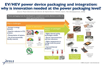
This explains the large variety of different approaches, which continue to co-exist, as regards power module design, power module packaging materials and manufacturing processes.
Most packaging solutions are strongly interlinked, and therefore, a holistic approach is being considered for the power module design, and, in the case of vertically integrated (module-inverter) companies, also for the inverter design. The global general trend is to reduce module inductance and to improve heat dissipation by using thin-profile power card-like modules, double side cooling (mainly with leadframe interconnections), structured baseplates for direct cooling or combinations of above.
Use of Si3N4 AMB ceramic substrates
We also need to examine how are Si3N4 AMB ceramic substrates used for high-power silicon and for SiC power modules.
Rosina said: “Si3N4 AMB is considered as the best performing solution for high-power-density silicon and SiC devices under challenging EV/HEV conditions, especially frequent thermal cycling. A clear trend toward using a triple winning combination (SiC die, Si3N4 AMB substrate and silver sintering die attach to the substrate) is being observed in the EV/HEV industry. However, other solutions also exist, at lower cost and “good enough” reliability.”
IMS benefits
Insulated metal substrate or IMS is for low- and mid-power devices being used. What are the benefits?
He added that the IMS is used mainly in the low-power devices, especially where high heat spreading is required. There is a lot of technology progress in this field, especially by Japanese players, but it is still challenging to increase thermal conductivity of an IMS dielectric sheet above 10 W/mK, while keeping IMS’ cost advantage compared to ceramic substrates.
Isn’t the use of silver sintering increasing? He said that the main reason is its superior reliability compared to more conventional soldering solutions, especially under EV/HEV operating conditions.
And, what about the interconnection technology being developed / used? Rosina elaborated: “There is a lot of development on low-inductance and more reliable interconnection methods, to get substitutes for conventional wire bonding solutions.
Leadframe/copper clip solutions are being increasingly used which enable lower inductance, enhanced reliability and improved heat dissipation. Such solutions are also better compatible with double-side cooling power module designs.”
Market size
Finally, what is the estimated market size over the next five years?
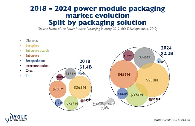
Rosina concluded: “The power module is one of the key elements in power converters and inverters. In fact, by 2024 EV/HEV will become the biggest power module market, representing a market value of almost $2.5B. In the past, power module packaging needs were driven by industrial applications, but today they are increasingly driven by EV/HEV.
“The power module packaging solutions developed initially for EV/HEV market are being increasingly deployed also in other applications. According to Yole Développement’s analysis, the global power module packaging market will reach $2.2B by 2024 representing thus a huge market opportunity for power module packaging companies and their material and equipment suppliers.”
Aspinity smart-sensing edge architecture tackles power- and data-efficiency problems
Aspinity, a semiconductor startup funded by Alexa Fund and others, and based in Pittsburgh, USA, recently announced the first smart-sensing edge architecture to tackle the power- and data-efficiency problems in the billions of battery-powered consumer electronics, smart home systems, and predictive-maintenance devices on which we increasingly rely.
Aspinity announced its reconfigurable analog modular processor (RAMP) platform, an ultra-low power, analog processing platform, that overcomes the power and data handling challenges in battery-operated, always-on sensing devices.
Incorporating machine learning into an analog neuromorphic processor, Aspinity’s RAMP platform enables 10x power savings over older architectures. Devices can now run for months or years, instead of days or weeks, without battery recharge or replacement.

Smart-sensing edge architecture
Elaborating on Aspinity’s smart-sensing edge architecture, Tom Doyle, CEO and founder, said that Aspinity offers a fundamentally new architectural approach to conserving power and data resources in always-on devices. The scalable and programmable RAMP technology incorporates powerful machine learning into an ultra-low power analog neuromorphic processor that can detect unique events from background noise before the data is digitized.
By directly analyzing the analog raw sensor data for what’s important, the RAMP chip eliminates the higher-power processing of irrelevant data.
System designers can now stop sacrificing features and accuracy for longer battery life. Aspinity’s analyze-first approach reduces the power consumption of always-sensing systems by up to 10x and data requirements by up to 100x.
The RAMP chip’s analog blocks can be reprogrammed with application-specific algorithms for detection of different events and different types of sensor input. For example, designers can use a RAMP chip for always-listening applications, where the chip conserves system power by keeping the rest of the always-listening system in a low power sleep state, until a specific sound, such as voice or an alarm, has been detected.

Unlike the other sensor edge solutions for voice activity detection, the RAMP chip also supports voice-first devices by storing the pre-roll data required by wake word engines.
For industrial applications, designers can use a RAMP chip to sample and select only the most important data points from thousands of points of sensor data: compressing vibration data into a reduced number of frequency/energy pairs and dramatically decreasing the amount of data collected and transmitted for analysis. This is the USP for the RAMP platform.
With so many ways to program a RAMP core, as well as broad algorithm support for different types of analysis and output, the RAMP chip uniquely enables a whole new generation of smaller, lower-cost, more power- and data-efficient, battery-operated, always-on devices for consumer, IoT, industrial and biomedical applications.
Much longer battery life
Short battery life makes always-on sensing devices unattractive. Will this change? Aspinity certainly thinks so! Doyle said manufacturers of battery-powered always-on sensing devices certainly want to improve battery life because users don’t want to have to frequently recharge or replace batteries.
Is this going to cut into battery suppliers’ revenues? He added that Aspinity does not remove the need to have a battery. Rather, it improves the battery life considerably, saving up to 10X battery in always-on sensing devices and up to 100x data. Thus, battery suppliers will still sell batteries; their batteries will last longer on a single charge (for devices that have rechargeable batteries). Device manufacturers may also be able to move to smaller batteries.
Demand for always-on sensing devices surging
Why is the demand for always-on sensing devices surging? For example, there are folks who may not appreciate this. Doyle noted: “People enjoy interacting with electronic devices in an untethered way (voice-first) – and they want this to feel natural. So, they want those devices listening all the time. They also want to have smart home devices that are wirelessly connected – and they want to have industrial machinery connected to wireless sensor nodes as well. This is the user interface migration story.
Finally, how does RAMP incorporate modular, parallel and continuously operating analog blocks that mimic the brain’s efficiency? Also, wasn’t this tried earlier? The patented and innovative RAMP technology enables sophisticated digital signal processing tasks to be replicated in analog.
Aspinity has leveraged the nonlinear characteristics of a small number of transistors to enable a new architectural approach to machine learning: modular, parallel and continuously operating analog blocks mimic the brain’s efficient neural network.
These blocks are configurable for typical analog tasks such as sensor interfacing, signal processing and data conversion as well as more complex tasks such as feature extraction, event detection and classification. Each one of these blocks is implemented in a much smaller footprint than a traditional analog block and allows early event detection from raw, unstructured analog sensor data.
Watch out for edge-emitting lasers (EELs): Yole
Last year, edge-emitting lasers (EELs) had represented a US$2.5 billion market, according to France’s Yole Développement (Yole), in its technology and market analysis. EELs are mainly used in optical communications, with optical systems for datacom and telecom.
Martin Vallo, Technology & Market Analyst at Yole Développement, France, said: “Growth is still driven by the optical communication market segment with optical systems for datacom and telecom. It is today the largest EELs segment with 56 percent of the total revenue in 2018.” The potential market size for EELs in future, is said to be worth $4.6 billion for 2023 at a CAGR of 13 percent.
Killer apps
Let’s find out the traditional applications that are still driving the EEL market. He said: “Growth of EEL market will continue to be driven by the optical communication segment, such as optical systems for datacom and telecom. This is the largest segment today for EELs, comprising 56 percent of total revenue for 2018. Material processing and display applications are also substantial, making up 16 percent and 14 percent of the market, respectively, in 2018.”

And, how about the potential killer applications that are emerging? Vallo said that the market shares of traditional application, particularly, optical storage, will decline in the future as 3D sensing in LiDAR, and face/gesture recognition, medical and lighting applications emerge in the next five years. Those might represent potential killer applications for EELs in the middle/long term.”
About specs
There are said to be too many different specifications for EELs. Elaborating, Vallo said: “Nowadays, laser technologies are ubiquitous in plenty of new applications. Since customers require turnkey solutions for their specific, for example, manufacturing process the leading players are capable to deliver many modifications from EEL device design up to the laser system.

“Generally, the buying process starts with definition of primary application – justification of interaction laser light with a matter. There are many application requirements from the laser technology and on the other side EEL has few basic designs that multiply the number of their technical parameters.”
Also, it seems each application needs its own, specific EEL technology. He added: “The primary reason is to deliver the best matching laser system for particular/each application. The differences in design don’t have to be significant necessarily but most of the time the parametrical changes affect the epitaxial process as well as front and process.”
Variety of designs available
The EEL industry is also showing a huge variety of possible designs. Expanding on this, he said that the combination of basic EEL designs such as Fabry Perot (FP), Distributed Bragg Reflectors (DBRs), Distributed Feedback (DFB) and Broad Area Laser Diodes (BALDs), and wide ranges of technical parameters, as well several types of packages, enable to deliver customized design for any type of application.
So, does all of this represent a challenging market for the industry ahead? Vallo added: “There is a large variety of applications, and system and device specifications, as well as a strong competitive landscape at the technology level, between direct diodes, fiber lasers, CO2 laser, DPSSLs and excimer lasers. The laser systems using EEL take the share of market of the CO2 and excimer lasers due to better efficiency.”
Specifically, what can the datacom industry do to establish leadership in EEL? As per statistics, optical systems for datacom and telecom represent the largest EELs segment with 56 percent of the total revenue in 2018.
EEL vs. VCSEL
Finally, are VCSEL and GaAs potential application areas as well? Else, what’s different? Vallo said EEL is an edge-emitting laser diode and VCSEL is a surface-emitting laser diode. Both are photonic devices made of GaAs. The difference is in the way of output beam propagation (EEL – from the edge, VCSEL from the top) and thus, in the design.
Gallium arsenide (GaAs) is compound semiconductor material, used to epitaxially grow, particularly IR (infrared) and photonic devices (such as LED, EEL, VCSEL, etc.). Infrared (invisible) emission is given by the physical material properties of GaAs.
He added: “EEL and VCSEL are used in transceivers – optical modules installed in the datacenters. VCSEL-based transceivers are used for short transmission distances up to 300 m with lower transmission speed (< 5 Gbps) whereas EEL-based transceivers reach long-haul distances with high transmission speed (~ 40-50 Gbps).
“Moreover, both EEL and VCSEL are key devices that can be used for 3D sensing applications – LiDAR, face/gesture recognition. EEL is more powerful due to its higher intrinsic (natural) emission brightness, which helps to extend the sensing range.”
— By Ms Aanchal Ghatak & Pradeep Chakraborty
Building up industry knowledge! For good!!
This is an old post from 2007. I am re-posting it, as per some requests. I have made minor changes. It is actually very useful to anyone who cares to read.
Fate has been most kind to me. Fate has also been most kind to me in terms of bringing me in touch with several good folks who appreciate whatever little talent I possess.

One of my good friends, Alfred Cheng, in Hong Kong, suggested that I speak to the sales team at Global Sources regarding building up the industry knowledge. It was an idea, floated later, by Claudius Chan too. I actually ended up taking a session with the team! 😉
May I also add that two of my very, very dear friends, Kevin Ho Lau Fai and Jo Yashan Kuo, felt great pride after reading my presentation, and later, thanked me profusely.
Well, it’s all worth it when you have friends such as these four, who take the time to appreciate all of your efforts. They make my day, my life! Thanks guys!!
Here’s what I have to say regarding building up industry knowledge.
‘Speaking’ the supplier’s language
- From experience, suppliers open up to those who can share information on their (suppliers’) industries/verticals.
- From experience, suppliers open up to those who can share information on other markets.
- From experience, suppliers open up to those who provide good, useful, suggestions.
- Suppliers DO NOT open up easily, if you cannot provide insights about specific verticals of their interest.
- Suppliers would respect you even more, if you could provide meaningful suggestions.
- Suppliers always look for leads; so, develop a habit of providing those.
- Suppliers also look for trust; provide that by exchanging relevant information, when possible.
- If covering electronic components, try and get an insight on the industry. It certainly helps!
- If covering electronics, computer or telecom, know the industry background a bit; see how a supplier laps up all the information that you may have.
- Convert the supplier into a trusted ally. How do you do that?
- Suppliers always look for leads; develop a habit of providing those.
- Suppliers look for trust; provide that by exchanging relevant information, when possible.
- Try and understand what the buyers need; it helps in understanding the suppliers needs.
- From experience, suppliers are keen to know what’s happening in India and China? Can you provide that information?
- Do not provide statistical information, as suppliers already have access to that! Instead, give them information you may have gathered from other sources.
- China and India markets are very strong cases. Develop yourself and know more about those.
Most of all, keep learning all the time.
Educate yourself!
No one can say, “I’ve a good knowledge about an industry.” Absolutely, no one! There is no end to learning!
Everyday, new things are happening. How do we keep pace with so many new things happening in the verticals? The best way is to educate yourself at work!
Education-at-work programs
Follow these religiously:
- Bookmark relevant Web sites – visit them often.
- Sign up for newsletters and news – at least, read the headlines.
- Flip through technology and other magazines you may get your hands on – there’s always something to learn.
- Build your network and get help.
- Visit Web sites of leading research firms, there’s lot of information out there.
- Visit Web sites of industry associations.
- Visit Web sites of industry events, look at the live coverage.
- Browse presentations of industry events; that’s an excellent way to track trends.
- Read relevant articles in print/on Web.
- If you don’t understand a technical term, do search on the Web/dictionary. You don’t need an expert, nor do you need one to tell you what the term means.
- Listen to what the suppliers say – you can pick up lots of points.
- Make it a point to talk to your seniors, especially in sales and editorial – they actually have a lot of information to share.
- Look up competitor Web sites and magazines – they always have relevant stuff.
- Read flyers and memos from sales and marketing departments.
DEVELOPING SOUND INDUSTRY KNOWLEDGE TAKES LOT OF EFFORT AND TIME! BUT, IT’S ALL WORTH IT!
PS: A leading manufacturer has launched next-gen ultracapacitors. While I won’t divulge who, it certainly took me back to my earlier posts. Again, if interested, read here.
