
Semiconductors
Bridging digital and physical worlds with efficiency and intelligence!
2024 IEEE Symposium on VLSI Technology & Circuits will be held June 16-20 at the Hilton Hawaii Village, Honolulu, Hawaii. The conference theme is bridging the digital and physical worlds with efficiency and intelligence.
Gosia Jurczak, Lam Research, and Borivoje Nikolić, University of California, Berkeley, are the Symposium Chairs. Takaaki Tsunomura, Tokyo Electron Ltd and Mototsugu Hamada, The University of Tokyo, are the Symposium Co-Chairs.
Vijay Narayanan, IBM T. J. Watson Research Center, and Ron Kapusta, Analog Devices, are the Program Chairs. Kazuhiko Endo, Tohoku University and Sugako Otani, Renesas Electronics Corp., are the Co-Chairs.

The plenary speakers are: Dr. Ahmad Bahai, CTO, Texas Instruments, on making sense at the edge. Dr. Maryam Rofougaran, CEO, Founder, Movandi Corp., on wireless and future hyperconnected world. Hidehiro Tsukano, Senior VP of R&D, NTT Corp., on photonics-electronics convergence devices to accelerate IOWN. Dr. Kazuoki Matsugatani, Senior Director, R&D Center DENSO Corp., on mobility evolution: electrification and automation.
The conference commences June 16 with standing workshop and three parallel workshops. The standing workshop is on advancing SoC design: open-source and ML-driven approaches in the cloud. Three parallel workshops are: novel metals for advanced interconnect, high-performance mixed-signal circuits: recent art balancing the analog vs. digital effort, and biosensory breakthroughs: pioneering the future of health tech.
June 17 has short courses on tech and circuit each, and a demo session. Circuit course is on circuits and systems for heterogeneous integration. Tech course is on advanced VLSI technologies for next-generation computing. Demo session, first introduced in 2017, has 15-20 demos.
June 18 has plenary talks, regular paper sessions, WIC and YP event, and an evening panel discussion. Joint panel for circuits and technology is on: Will AI bite the industry that feeds it? It will be moderated by Tokyo Institute of Technology. There will be seven participants from Qualcomm, KLA, SK Hynix, imec, Nvidia, KAIST, and Stanford University. There will be a game-show like competition between chip heroes (panelists and audience) and gen-AI.

There will also be Women in Circuits & Young Professional Mentoring event, Test of Time award, VLSI Symposia Best Student Paper award (BSPA), with a winner each for circuits technology, and Best Demo Paper award. June 19 has plenary talks and regular paper sessions.
June 20 has regular paper sessions and luncheon talk. Luncheon talk will be on CHIPS Program and you: an R&D update for VLSI symposia. It will be delivered by Greg Yeric, Director of Research, CHIPS National Semiconductor Technology Center Program, CHIPS R&D Office, US Department of Commerce.
There are 17 technology sessions, such as oxide semiconductor applications in BEOL, backside of silicon: from power delivery to signaling, NVM — Hafnia-based ferroelectrics-1, novel channel materials for advanced CMOS, etc.
There are 29 circuits regular sessions, such as wireline circuits, power at high voltage and current, AI/ML accelerators and CiM, biomedical stimulation and imaging, etc.
There are six joint focus sessions, such as RF, mmWave, and THz technologies, processors and compute, thermal management and power delivery in 3D integration, biomedical technologies, image sensors, and memory-centric computing for LLM.
VLSI 2024 will see historical high for paper submissions, totaling 907. 41 percent of the accepted papers are from the industry. The USA and Korea have the highest number of accepted papers, followed by China and Taiwan. Other countries include Japan, Belgium, Singapore, France, Switzerland, etc.
CHIPS metrology NOFO on small business innovation research (SBIR) announced
CHIPS Metrology NOFO on small business innovation research (SBIR) was held recently in USA.
Marla Dowell, Director, CHIPS Metrology Program said CHIPS Metrology catalyzes innovation with an emphasis on accurate, precise, and fit-for-purpose measurements for producing microelectronic materials, devices, circuits, and systems. The mission is: measure, innovate, and lead to enhance a vibrant US ecosystem for semiconductor manufacturing, and promote US innovation and industrial competitiveness.
Goals include: expanding measurement solutions for semiconductor ecosystem, increase the number of solvers by harnessing diversity of people and ideas, inside and outside of NIST, and expand education and workforce development opportunities that inspire excitement about manufacturing careers, and expand career pathways.

SBIR program
Sarah Hughes, Chief of Staff, CHIPS Metrology Program, stated that SBIR program encourages domestic small businesses to engage in R&D, with potential for commercialization. It stimulates commercialization of technological innovation from private sector through federal R&D funding. It can foster participation in innovation by socially and economically disadvantaged small businesses. Federal agencies with extra-mural R&D budgets exceeding $100 million are required to participate. Agencies determine the R&D topics in their solicitation or Notice of Funding Opportunity (NOFO).
For eligibility, small business concern should be for-profit business located in the USA. They should be more than 50 percent of equity owned and controlled by one or more individuals who are US citizens or permanent residents. Other for-profit small business concerns should be owned and controlled by either US citizens or permanent residents. They should have no more than 500 employees, including affiliates.
Funding amounts are up to $283,500, with an additional $6,500 for technical and business assistance in phase I. Phase II will have up to $1,910,000, with up to $50,000 for technical and business assistance. Period of performance ranges from 6 months, with one month allocated after to prepare and submit a final report for Phase II funding consideration, in phase I. Phase II is up to 24 months.
Technical and business assistance (TABA) details that funding opportunity included in SBIR award to help small businesses commercialize their technology, by either funding vendors directly, or providing funds to small business awardees to contract their own vendors or consultants. NOFO has more details on how and when awardees can apply for TABA.
By Jun. 14, 2024, full applications must be received at Grants.gov office. NIST application review, selection, and award processing takes place from Jun-Aug. 2024. Sept. 2024 is anticipated the earliest start date for awards under this NOFO.
Dean Iwasaki, Grants Officer and Team Lead, NIST, listed CHIPS Metrology grand challenges. These are:
GC1 — Materials purity, properties and provenance.
GC2 — Advanced metrology for future manufacturing.
GC3 — Metrology for advanced packaging.
GC4 — Modeling and simulating semiconductor materials, devices, and components.
GC5 — Modeling and simulating semiconductor manufacturing processes.
GC6 — Standardizing new materials, processes, and equipment.
GC7 — Security and provenance of micro-electric components and products.
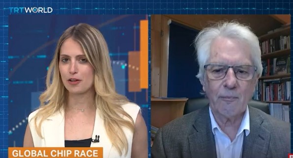
Japan needs to put their mind, and bridge semiconductor gap, China in catch-up mode
TRT World is a Turkish public broadcaster. In Money Talks, a TRT World production, it was reported that the global semiconductor market is expected to grow 13.1 percent to $588.36 billion in 2024.
Memory chips are anticipated to lead with 44.8 percent, driving market growth. Next, Americas is expected to grow by 22.3 percent, and Asia Pacific by 12 percent in 2024. TSMC, Nvidia, Samsung and Intel are expected to lead the global AI chip trends.
Malcolm Penn, Chairman and CEO, Future Horizons, told Money Talks about the importance of semiconductors, and its impact on the stock market in the near future. He said memory has always been an importance segment of the semiconductor industry. It generally accounts for a quarter or a third of the overall sales. What happens in memory affects the overall semiconductor market.
Memory has seen a down-cycle for the last two years. It is now on upside, and recovery will be very strong. It is also the driving force behind the overall recovery we are seeing. The other parts of the semiconductor market, including discretes, have been growing in single digits so far. We are seeing a memory-led recovery. Memory is always the first into the downturn, and first into the upturn.
Regarding the chip war among China, Taiwan, and USA, he added that China is always playing catch-up in terms of technology, which is quite normal. New regions are entering the semiconductor market. It will take time to catch up. China has got two or three nodes in leading edge. China has aspirations for Taiwan. That led the rest of the world to see what can be done to stall China’s entry into Taiwan, and in the high end of the market. That led to the current restrictions on China, led by America. There is this move to push China back, and try to slow it down. They want to keep the lead with TSMC, in particular. The whole world depends on TSMC.
Japan saw modest growth of 4.4 percent last year. How can it maintain growth? Penn noted that Japan was very strong in the 1980s. It was steaming ahead in technology, manufacturing, etc. They have gone from 28 percent share of the global semiconductor market to just 8 percent. They have lost of lot of their OEM segment, which was the market for semiconductors. They have also fallen back in technology.
Japan is now making a very brave effort right now to pull back and catch up. They are certainly doing very well. They have some very good investment projects going on. But, that’s not going to happen overnight. There are huge factors in the equipment industry, huge factors in the materials industry, etc. Japan now has the pieces in place. They need to put their mind to it, and bridge that gap.
Innovative technologies for sustainable future of semiconductor industry: IRPS 2024
IEEE International Reliability Physics Symposium (IRPS) 2024 was held in Dallas, Texas, USA. Su Jin Ahn, EVP, Advanced Technology Development Office, Samsung Semiconductor R&D Center, presented the plenary on innovative technologies for sustainable future of semiconductor industry.
Semiconductor market growth will be from $224 billion to $350 billion for computing and data storage. Automotive electronics has moved to $150 billion. We are seeing an explosive growth of data and rapid development of AI. Data creation is accelerated by GenAI. We had AlphaGo, developed by London-based DeepMind Technologies, an acquired subsidiary of Google, in 2015.
Today, we are witnessing growth of wafers and semiconductor fabs. Number of fabs using 300mm wafers has increased x3 over last 15 years. There is paradigm shift in computing over the past 80 years. From mainframe era, we have now come hyper-scale connectivity and AI. Moore’s Law-based geometry scaling has been at the heart of all these developments. We have seen evolution of photo-lithograph, multi-patterning, etc. There has been structure and materials innovations as well. There is changing landscape of memory and logic devices in IRPS papers. Reliability issues need to be overcome for new structures and materials.

We are seeing evolution of backend-of-line metals. We have relied on low resistivity and high reliability for performance, speed, and power efficiency of chips. There is evolution of NAND flash memory. It is now entering 3D stack up and WF bonding. Stacking has moved to heterogenous integration. There are mutual thermal, chemical, and stress effects. There are potential reliability issues. Cell-to-cell variations from top to bottom increases due to deep contact hole. There are stress-related problems in wafer bonding.
Technologies in works
We are now in logic scaling trend. CPP scaling has slowed down due to short channel effects, and contact resistance. Cell height scaling slowed down due to rising metal resistance. We have prospects for logic transistor beyond planar TR. We moved from planar TR to FinFeT at 14nm. At 3nm, we have the gate all-around (GAA) MBCFET. At <1nm, we have 3DS FET and CFET.
We have potential reliability issues in GAA transistor. Thin body and process complexity degrade HCI. Structural complexity and increased packing density is vulnerable to heat dissipation. For self-heating, we can maintain temperature at thin nanosheet channels.
We have potential reliability issues in 3DS FET. Accumulation of process damage causes TDDB, and BTI degradation. Complex 3D layout causes Vth variation, and self-heating deteriorates. We also have potential reliability issues in 2D channels. We have to look at material quality, full integration into logic process, defect control, etc.
We have prospects for DRAM cell beyond 10nm. Area scaling continues via vertical channel transistor or vertically-stacked cell array. Potential reliability issues include an undesired hole accumulation in thin floating channel that increases the sub-threshold leakage. Beyond Si-channel, we have deposition-able IGZO channel transistor in vertical channel transistor (VCT). We also have potential reliability issues in IGZO channel. There can be thermal instability in process integration, abnormal PBTI, and ion-Vth trade-off behavior.
Future prospects
In future, we will be transitioning to 3D stack era. We will move to cell array and periphery circuit, and heterogenous integration. We are moving to wafer bonding and advanced packaging. We are seeing the evolution of package technology. We are pursuing fine pitch bonding (<2um) for interconnect density (>2e5/um2) compatible to SoC. We are moving to wafer-to-wafer and multi-chiplets.
There are potential issues in 3D-IC. These include massive bonding interfaces (multi-chiplet, multi-stage HBM) that increases EM risks. Pitch scaling and low temperature process weakens bonding interface stability.
There are several future reliability challenges. They include TDDB, EM, FBE, HCI, BTI, self-heat, etc. Thanks to new semiconductor technologies being developed, we have managed the challenges well, so far. More is expected in future.
New leaders can capture the chiplet revolution
TechInsights, USA, organized a fireside chat today on the global semiconductor industry.
G. Dan Hutcheson, Vice Chair, TechInsights, said, the Chinese economy has been starting to recover now. We are also getting into a new PC up-cycle. Companies are also trying to move their centers of excellence to the other countries. We are seeing a normal upside right now. You do get some variation in supply over the period of 12 months. We are also moving into the 2nm era next year.
The magnificent seven for everybody includes: Apple, Amazon, Google, Meta, Microsoft, Nvidia, Tesla, etc. Microsoft and Apple came out of the PC era. Amazon and Google came out in the 2000s. Nvidia came out of semiconductors. Tesla happened later. Apple is still riding on the smartphone. We also have the growing EV market. AI has also been emerging strong. However, AI stocks were worst performing among semiconductors stocks last week.

Nvidia has done a double lock-up recently. It has GPUs and whole system. They are re-architecting the way the data center works. Nvidia is, where it is today. We now need a new technology to be the next big thing. When Apple iPhone first came in, it started a new revolution. It always surprises you!
We will have new leaders in future. We will also see new leaders capturing the growing chiplet revolution. The foundries that exist would not have been possible without the EDA revolution. Chiplets have now emerged as the new revolution.
We have neural network processors already. We also have cellphone APUs. There are some really cool things coming that will help organizing your life, especially using the smartphone.
AI is seeing huge explosion in entrepreneurial pursuit. Several AI chip startups will be coming up. GPUs always had an innate advantage. GPUs chips were power hungry. We now need to partition that down to smaller parts. PCs had closed architecture partnership between Intel and Microsoft. We later saw the explosion of innovation around apps. AI is more of a curiosity right now. IBM used it to help physicians diagnose cancer. Today, it has become routine. AI solutions will take step forward, and bring real value.
China needs to catch up
As for domestic Chinese companies in AI, China is developing its own core technology. Taiwan has been incredibly successful as it has access to the global technologies. China also needs to do lot of classical innovation to get forward. Doing a lot of innovation can be very cultural. Silicon Valley is one example to follow. We are hoping that China can catch up, and get back to the order, and we can get back the global order.
AI will be used on chips to improve MCU/MPU performance. Synopsys is a world leader that enables all of that. We are also seeing new process technologies being developed. However, we still need the human intelligence to make all of this happen. AI, as a tool for engineers, may make them struggle. People were locked into their tools earlier. You have to be really good at using all the weapons at your disposal. If you don’t, you can be left behind. We are also going to go through another productivity surge in future
Regarding alternatives to silicon, he said that God was bullish on silicon. It has proved to be the best material. Today, we have substrates with specific functions. We have to get around the interconnect level. Data centers are migrating further down to the new chips. Quantum does replace it! However, it will co-exist with silicon.
Lead times are delivered largely by the complexity of the problem addressed. Today, we have about 2,000 process steps, but the lead time is still 12-13 weeks. We have to address complexity. We had the case of just-in-time. We may create disaster if we moved to just-in-case. Shrinking lead times requires you to decrease utilization. We saw lead times decrease to 60 percent, using utilization. Intel had increased utilization by increasing hot spots.
We also need to look at the supply chain. As we become more efficient, we may also be dealing with even more complexity. We cannot see that either happen, or decrease, in the forseeable future. Regarding NAND demand, we are witnessing the incoming demand, at least from data centers.
Japan getting back mojo!
Finally, which country can emerge as a semiconductor powerhouse? Japan is finally getting over lost decades. Japan is coming back certainly. It appears that Japan has got back its mojo after a long time. China is also going to grow. India has an advantage of cheap labor force. India may have difficulty in duplicating the success of software. It has advantages and disadvantages.
Japan and South Korea are much ahead right now. The US recovery is also taking place. Mexico is starting to rise. That’s driving new factories inside Mexico. Canada has a liberal immigration policy. Some of the best and brightest are present there. There is always opportunity. With technology, you need to run faster, work smarter, etc.
He hoped that everyone is safe in Taiwan, following the earthquake. Despite the severity of the tremors, the impact on Taiwan’s semiconductor manufacturing capacity appears to be limited. TSMC has done, and been doing incredible work in the future.
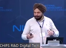
CHIPS R&D workshop addresses digital twin data interoperability standards
Digital twins in manufacturing enable proactive decision-making, predictive maintenance, scenario testing, and collaboration among stakeholders, etc. This workshop will focus on standards needs for a specific use case, application of a digital twin for manufacturing in the chiplet-packaging module.
CHIPS R&D, USA, organized a conference today. Participants discussed the potential for digital twin technologies to drive progress in the semiconductor and microelectronics industry. They looked at the role of data interoperability standards for digital twins in semiconductor manufacturing ecosystem.
Factors to be considered in identifying standards priorities include potential for broad impact, feasibility for accelerated development, and suitability for various standards development channels, including through alliances, incubators and accelerators, and standards setting organizations.
CHIPS Manufacturing USA
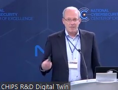
Eric Forsythe, CHIPS R&D, provided an introduction to CHIPS Manufacturing USA. We have a funding opportunity and context. CHIPS Manufacturing USA falls under the CHIPS Act. We will try and solve problems, specifically for the digital twin. We have a workforce initiative going on, as well. We are focused on workforce development. Within the R&D portfolio, we have Natcast, NAPMP, CHIPS Manufacturing USA, with 17 institutes across the network, and CHIPS metrology program.
Manufacturing USA purpose is to accelerate the discovery to US production. We are creating an effective collaboration for applied industry research to bridge the gap from discovery to production. The process has basic research, proof of concept, production in lab, capacity to produce the prototypes, capacity in the production environment, and the demonstration of production rates.
We have minimum NIST commitment of ~$200 million over a five-year period. We are analyzing RFI responses, industry feedback etc., for digital twins. The objectives include reduce time and cost for chips development and manufacturing. Accelerate adoption of the semiconductor manufacturing innovations. We are also increasing the access to semiconductor manufacturing training, etc. We have established the shared resources capabilities, competitively fund industry-led technical and workplace development projects. We have digital framework for interoperable data, shared and validating data, etc. We are also creating a shared marketplace of digital twins model.
Digital twins in semiconductor manufacturing standardization
There was a panel discussion on defining the landscape, scope, and focus of digital twins in semiconductor manufacturing standardization efforts.
Kemaljeet Ghotra, Enterprise Data Strategist, PDF Solutions, said digital twin is a virtual representation of the physical world that is capable of producing intelligent feedback with simulation, emulation, data analytics, and modelling.
We are now developing virtual process, tools and devices, and virtual fab. Data is the horizontal across all. We have grand challenges such as generating data, create models, share, and use data, with security around it. Digital twin framework requirements include DT re-usability, interoperability, validity and verification, maintainability, capability, extensibility, accuracy, security, provenance, hierarchical relations, historian model life cycle, etc.
We need to have an operationally focused digital twin for the extended semiconductor supply chain. We need to bring in the end-to-end traceability for products. Operational DT allows for centralized management of globally distributed supply chain to be built on PDF’s Extensio platform capabilities. We need to allow sharing of data in much more secured environment.
PDF has AI models for automation and real-time insights for DT. We have added fault detection and classification, predictive maintenance, virtual metrology and sensing, and fab predictive model in the PDF solution. The operational DT leverages and expand PDF’s existing solutions and market presence. Focus is to get off different proprietary data types to be able to talk to each other.
James Moyne, Research Scientist, University of Michigan, stated that the scope of DT is across the manufacturing ecosystem. We have existing DT solutions. New ones are emerging from improved ecosystem integration, and solution integration. We also have improved reuse of solutions.
Enabling collaborative DT environment across the industry requires agreement on specs for DT and DT framework. DT is a purpose-driven digital replica of physical asset, process, system, or product. It quantifes prediction and prediction accuracy. The DT framework involves aggregation and generalization examples.
We need to understand requirements driving DT and DT framework definition. We have already done lof of work to identify requirements. We have a path forward for getting results into industry practise, such as International Roadmap for Devices and Systems (IRDS), SEMI, and other standard organizations.
Ben Davaji, Asst. Prof., Northeastern University, stated that development of targeted domain-specific DTs could be more efficient. DT for semiconductor manufacturing includes manufacturing process — such as drifts, aging, tool PM, diagnostics, etc. We can accelerate process development and characterization for manufacturing equipment. We can develop new process equipment and reduce evaluation times.
We can enable fast adoption of novel and emerging materials and substrates. We can do innovation in process design to enable novel device architectures. We can enable accelerated PDK development, etc.
DT for nanofabrication involves DUV lithography process and plasma etch process as examples. He talked about DNN-enhanced virtual metrology. We can have minimum viable DT with data standards, quantitative and multimodal data, TCAD and EDA to generate large data sets and calibrate using experimental data.
We can have DT black box from tool manufacturer and material suppliers. We can develop process and test datasets. We can have computational infrastructure to support secure computing and federated learning. We can also have an open environment for the integration of DTs, enabling interconnections.

Serge Leef, Head of Secure Microelectronics, Microsoft, we have been witnessing the convergence of electronics and physical worlds. DT was limited to chip-level modeling and simulation. We are seeing computing continuum up to 2030.
Modern systems are domain specific, highly heterogenous, distributed over networks, highly interactive with physical world, etc., and everything really has to work together. Physical prototyping for complex systems is a huge task. Typically, one or two prototypes can get built. We also need to have DT simulation, with heterogeneity challenge.
We now need to execute meaningful scenarios at near-real-time speed at near-zero modelling cost to gain actionable insights. Microsoft has developed vision for automotive and aerospace DTs. There are some walls between disciplines that need to be broken down.
Cloud-based architecture is leveraging speculative parallelism. We need to use ML to train reduced order models on real-world data. We have standards opportunities for simulation backplanes, modeling interfaces, and testing frameworks.
Gurtej Sandhu, Principal Fellow and CVP, Micron Technology, noted we have an end-to-end Si virtual model. DT of chip fab is virtual model of the entire process flow to accelerate technology development and ramp to inline and packaging yield.
Cost of developing chips is increasing exponentially. Tools are needed to make more informed decisions and build faster process flows. Successful collaborations require multi-disciplinary collaboration across the entire framework of chip building discipline, structure and materials, etc. Achieving this requires breakthroughs in multi-scale modelling. We also need partnerships among chip makers, tool providers, etc.
We have the fab technology co-optimization (FTCO) framework. We can have DT models on the top. It can be followed by metrology, process, tools, efficiency, and partners. A module-level co-optimization requires over 20 process steps/modules. A typical fab co-optimization requires over 1,000 steps. The DT platform is a virtual test bed. Members can develop tools/models, access data for testing/validation, and deliver DT solutions.
Victor Zhirnov, Chief Scientist, Semiconductor Research Corp. (SRC), talked about DT for microelectronics. SRC is creating CHIPS Manufacturing USA Institute. SEMI is partnering with SRC. DT should have plug-and-play capabilities. It is a tool for rapid innovation enablement. The MAPT plan is call for DT infrastructure.
We need to look at data standards that can be applicable for electronics manufacturing, We are quite familiar with design automation, modelling and simulation, and industrial automation.
Standards must be set to enable interchange of materials and 3D data between various entities involved in SIP design and manufacturing, Key drivers include multiple physics field nature of design. DT interoperability is currently a problem. We need universal standard to cover use cases.
CHIPS R&D semiconductor supply chain trust gets essential!
CHIPS R&D Semiconductor Supply Chain Trust & Assurance Data Standards Workshop started today in Rockville, Maryland, USA.
As semiconductor products are manufactured, key transactions are captured as data in different digital twin ecosystem modules (e.g., raw materials acquisition, design, layout, tape-out, mask making, chip fabrication, testing, packaging, and assembly). Digital twin modules must be linked together to allow backward traceability across these ecosystems, and to enable access to accumulated supply chain data for traceability, authentication, and provenance tracking.
Yaw Obeng, CHIPS R&D, welcomed the audience. He also introduced the Workshop Planning Committee.
Addressing supply chain issues
Carl McCants, Special Assistant to DARPA Director, presented the opening keynote on DARPA’s history in the semiconductor supply chain trust and assurance standards. It has been focused on addressing supply chain issues. We had a grand challenge in 2005, where we wanted autonomous cars. We had failed back then.
DARPA has been creating breakthrough, paradigm-shifting solutions. We are accepting and managing risks as well. Concern with globalized microelectronics ecosystem has also been addressed within DoD since 2000. DARPA TRUST and IRIS programs developed the techniques for validating design and process integration before distribution.
He also talked about EDA and testing, and whether the tools were doing what they were expected to do. For IRIS, we focused on what’s happening to the manufacturing process. DARPA SHIELD will develop the facility to provide 100 percent assurance against certain known threat modes quickly, and at any step of the supply chain.
Semiconductor manufacturing supply chain needs to address trust and assurance challenges. We need to maintain the confidentiality of the technology delivered, protect the IP, and have continuous and sustained access to technology needed. We have challenges such as data and definitions, so that a semiconductor product can be delivered without compromise to the product’s integrity, trustworthiness, and authenticity.
For IP protection, we need to incorporate, verify, and validate an IP into design. We need to protect the logic design and simulation of the chip. We also need to be able to transmit and store the functional test programs to the wafer fab facility, and the assembly, packaging, and testing facility. We also have to do aggregation of package-level test data in the APT facility, and take that to the customer.
Model and simulate semiconductor supply chain
Eric Forsythe, Technical Director, CHIPS R&D, introduced the CHIPS Manufacturing USA. The grand challenge is to seamlessly model and simulate the entire semiconductor supply chain. We need to create an effective collaboration environment for applied industry research to bridge the gap from discovery to production.
CHIPS Manufacturing USA Institute is meeting the digital twin institute objectives. These are: reduce time and cost for chip development and manufacturing, accelerate adoption of semiconductor manufacturing initiatives, etc.
Data — reliable, secure and accessible, workforce development, and model development and validation, were the top three areas to look at. These are the big challenges for developing digital twin technologies for semiconductor manufacturing.
Electronics supply chain digital security standardization
There was a panel discussion on landscape, scope, and focus of electronics supply chain digital security standardization efforts. The participants were Gretchen Greene, NIST, Chris Ritter, Idaho National Lab, and Christophe Bégué, PDF Solutions.
Gretchen Greene, Group Leader, Data Science Group, NIST, said we are currently building trusted chip environments (TCE). We are modernizing the ecosystem and leveraging digital technology. Security and interoperability remain the main issues.
In the CHIPS supply value chain, there are design, fabrication, package, assembly, and test, and commercial sectors. These are addressed by players in muti-physics and modelling, IP, Open Source, manufacturing process and tooling, materials and resources, photonics, microelectronics, etc.
Granularity of the semiconductor supply chain is at the heart of the standards challenge. The interoperability at scale supporting coarse grain digital assets has been inconsistent, and even non-existent. We have the opportunity to impact the industry. We are opening several windows of commercial opportunity for marketplace innovation.
We are also standardizing protocols, such as information sharing, smart connections, etc. We are making protocol specs, payload types, synchronization or process flows, status, managing authorities, verification/validation and resolver services, and registry/curation for monitoring, nodes/hubs, etc.
We are also developing a knowledge network via CHIPS exchange. Semiconductor knowledge can be shared across digital assets, such as taxonomy, machine, actionable, analytics, visualization, etc.
We have goals such as federate across supply chain through use of digital architecture connecting generations, standards, TREs and stakeholders. Strengthen exchange, reuse, and interoperability. Enable discovery and access, etc.
Digital engineering mission
Chris Ritter, Idaho National Lab, said that we have the digital engineering mission. Digital engineering transforms the way we design and operate energy assets. Digital engineering is an innovator and key success driver across all initiatives. It is a key enabler for net-zero program.
With DE, we can design — it links facility information. Operations enable the digital twin. He talked about Deep Lynx, its virtual, and physical platforms. Deep Lynx open source model is a centralized digital twin data warehouse and live event system. Ontological and time series storage of digital twin data streams is there. Event system can push and pull data in real-time around a digital twin. It is proven in operation of MAGNET digital twin.
Idaho National Lab has open ontology for thread and twins. General entity model (GEM) is an extensible, upper-level ontology. It has an advanced manufacturing app. It has digital twin demonstrations across lifecycle stages.

Supply chain traceability
Christophe Bégué, PDF Solutions, said the semiconductor market is currently looking at reliability, RMA or failures in the field, security, and regulation.
Supply chain traceability can provide fast and precise analysis of a reliability or security issue. We can enable short- and long-term containment plans to reduce cost and preserve brand. We can have assurance and preferred supply through provenance and traceability.
We need standards for single device traceability. We have SEMI E142 standard that defines a data model for devices within a wafer or complex assembly. Devices have a virtual identifier (VID) based on this model. E142 forms basis for single device tracking.
We need standards for supply chain traceability. SEMI is developing Specification for Supply Chain Traceability using Distributed Ledger Technology standard proposal to record chain of custody and provenance. We also have SEMI Supply Chain Traceability using distributed ledger technology or DLT. Standard currently defines the data and transaction model, asset lifecycle, and services.
Using diamond films to enhance thermal performance in electronics packaging
IEEE Electronics Packaging Chapter, Santa Clara Valley Chapter, USA, recently organized a seminar on using diamond films to enhance thermal performance in electronics packaging.
Artificial diamond films are deposited from a mixture of methane and hydrogen — and the deposition of the material is not an expensive process. However, the integration of diamond films and electronic devices requires the development and optimization of new processing lines, which is a costly procedure. LEDs, for instance, have become low-cost components.
Dr. Joana Catarina Mendes, Researcher at the Instituto de Telecomunicações in Portugal said a diamond is metastable allotrope of carbon, where carbon atoms are arranged in a variation of the face‐centered cubic crystal structure known as diamond lattice. It has small atomic radius, extremely strong covalent bonding between sp3 hybrid orbitals, and set of extreme properties. Some properties include high hardness, high demand inertness, high young modules, high thermal conductivity, high bandgap/breakdown field, high electron mobility, and low dielectric constant.

Natural diamond forms 150-200 km inside the earth’s mantle under extreme conditions. Despite their high commercial value in jewelry, natural diamond crystals have too many defects, and cannot be used for electronic applications. Their use is typically limited to tri-bological apps.
Diamond synthesis
Artificial diamond can be formed under high pressure and high temperature (HPHT). The HPHT method reproduces diamond formation conditions inside the earth’s mantle. Diamond seeds are placed at the bottom of a press at 5 GPa. The internal part of the press is heated above 1400°C, and melts the solvent metal. The molten metal dissolves and drags atoms from high purity carbon source, which precipitate on the diamond seed.
Another method is chemical vapor deposition (CVD). CH4 and H2 are typical input gases. The input gases are dissociated and activated. The activated radicals flow and react with C atoms on a substrate. Atomic H etches away non‐sp3 C bonds. Due to their short wavelength (12 cm at 2.45 GHz) the MW power can be supplied as TEM or TM waves. Conductive plasma replaces the outer conductor of coaxial line in plasma discharge region.
Single crystal diamond (SCD) substrate leads to homoepitaxial diamond films. They have the highest thermal conductivity. They are ideal for electronic devices and thermal management apps. Non‐diamond substrate leads to heteroepitaxial/polycrystalline diamond films (PCD). Here, different substrates are possible, such as Si, SiC, GaN, etc.
Diamond films enhance thermal performance in electronics packaging
We can use diamond films to enhance thermal performance in electronics packaging. We can start by integrating diamond and GaN high-electron-mobility transistors (HEMTs). In some cases, the amount of heat generated per unit volume is comparable in magnitude to that encountered at nuclear reactors and at the surface of the sun! We need to cool down the hotspot. We can also grow diamond on the back of GaN wafer.
Next, we have capping diamond, where, films are deposited at 700°C. Metal heat spreaders transfer the heat to the underlying HEMT holder. Thermal resistance is reduced by ≈ 40 percent, and junction temperature is lowered by 100°C @ 25 W/mm. 4’’ GaN‐on‐diamond wafer volume manufacturing was achieved in 2021. Radios and power amplifier modules are available for satellite apps.
Diamond substrate needs GaN/diamond wafer bonding. We can do thermocompression using adhesive layer, as well. We can also do surface-activated bonding (SAB). Another method is Van der Waals (VdW) bonding. The process was initially employed for GaAs thin films.

Other uses
Diamond can be used as chip‐carrier of power LEDs. We can also have diamond carriers for high power LED dice. Diamond can also be used as power board. Depending on the activation energy of the aging processes, LEDs mounted on diamond board will age 60-90 percent slower @350 mA and 90-99 percent @700 mA.
Conclusion
Diamond has been successfully used to improve the thermal management of different devices.
For GaN HEMTs, we have diamond‐capping of passivated HEMTs, direct growth of diamond on back of GaN wafers, bonding of GaN wafers/HEMTs and diamond substrates, commercial GaN‐on‐diamond‐based RF power amplifiers are available for satellite communications. Companies such as Mitsubishi Electric Corp. and Fujitsu are involved in research.
Diamond as chip‐carrier has similar impact of PCD and SCD carriers on LED characteristics. It improves stability of the wavelength with the current, and increases LED lifetime significantly. Diamond as power board increases LED lifetime considerably, when compared to standard MCPCBs. The results can be extrapolated to other devices.
What’s happening with current and future chiplet security?
Electronic System Design Alliance (ESDA), part of SEMI, USA, organized a conference today on chiplet security — current and future.
Many semiconductor-based systems are moving toward 2.5D and 3D designs consisting of different pre-manufactured chips (chiplets) that perform specific functions. These are often provided by multiple vendors, and are typically interconnected using an interposer.
However, unlike monolithic multi-function chips, chiplets can be developed anywhere and at any process node. As such, chiplets from untrusted vendors can be unreliable or malicious. Third parties can reverse engineer, overproduce, or steal the IP of chiplets. Consequently, they raise new security challenges for an industry still figuring out ways to effectively mitigate hardware security threats to monolithic chips.
There are potential threats at different stages of bringing chiplets to life, including design, assembly, and testing. The panelists assessed current safeguards to mitigate these risks and discussed open challenges for the industry and academia.
Bob Smith, Executive Director, ESD Alliance, the SEMI Strategic Association Partner, welcomed everyone, and introduced the panelists.
The panelists were: Serge Leef, Head of Secure Microelectronics, Microsoft, Dr. Swarup Bhunia, Semmoto-endowed Prof. and Director, Warren B. Nelms Institute, Salman Nasir, Senior Technical Program Manager, Battelle, John Hallman, Digital Verification Technology Solutions Manager, Siemens EDA, Ming Zhang, VP of R&D Acceleration, PDF Solutions, and Steve Carlson, Director/Solutions Architect, Aerospace and Defense Solutions, Cadence Design Systems. Raj Gautam Dutta, CEO, Silicon Assurance, was the moderator.

Chiplet security
Serge Leef, Microsoft, said that you need to think about chiplet security in two or three layers. Supply chain, side channel attacks, reverse engineering, are very important. Chiplets should have protection against these on board. Interposer presents opportunities and challenges. It can also hold secrets as it is manufactured as part of a chip. There needs to be security architecture across HI. We need to be aware of what should be of architecture.

Salman Nasir, Battelle, said we are witnessing a shift in the semiconductor industry. We are looking at security architectures of chips and chiplets. HI packaging is added to the chiplets. We also have to look at the security architectures. New measures can be included in the protocols, cryptographic accelerators, etc. Supply chain security is also imperative. We need to closely monitor the security.
John Hallman, Siemens EDA, added that we are looking at trust, verification, etc., in the chip. We need to take this from SoC to chiplet security. Malicious circuitry may go into early design. We need to have good start, with integration and verification. We need to also combine that with traceability or supply chain. We also need to protect IP against reverse engineering.
Steve Carlson, Cadence Design Systems, noted that we need to look at confidentiality, protection gains, access points, etc. It is a team sport across hardware and software,

Dr. Swarup Bhunia, Warren B. Nelms Institute, said chiplet security and integration is very important today. Now, SMEs can integrate diverse apps into a chiplet, and make that very democratic. Chiplets are individual ICs at a small scale. Side channel leakage, access control, etc., are areas to look at. Chip-level security can scale at package level. Also, the inter-chiplet communication can be a heavy attack surface. We need to think of new mode of inter-chiplet communication. Third, we need to create trustworthy chiplets, rather than using untrustworthy chiplets.
Ming Zhang, VP of R&D Acceleration, PDF Solutions, said there are unique things about chiplets regarding security. One, technology angle, and two, business angle. From technology side, chiplets have many interconnects, such as power, etc. The surface attack area could be larger. From business side, chiplets are seeing HI.
Different from SoC security?
How is chiplet security different from SoC security? Salman Nasir said they are quite similar. From an SoC perspective, you can oversee the process from design to manufacturing. The integrator has greater potential to address vulnerabilities. Third-party IP is a black box, and IP integration takes place at the foundry. On chiplet side, there are similar concerns. The first is trustworthiness of the chiplet. It’s a hot topic right now! We have Cyber Trust Mark Program, GSA has ties with IoT, and NIST is looking into this. We can also look at security measures for encryption, etc., to ensure architecture is confidential and unaltered. More will come in the near future!
Leef said the similarity is there. Side channel leakage, creating low emission cryptography are there, along with ML for anomalous communications, etc. Interposer-based architecture means that the interposer communications infrastructure could get exposed. We can shift the secrets to a trusted facility in the USA, such as routing tables, etc. NIST is also looking at standards to adopt.

Steve Carlson added that IP access across the ecosystem should be conducted carefully. We have a competitive commercial environment, and a lot is at stake there. Security has the most relative cost, and is not free.
Future challenges
Talking about challenges, Dr. Swarup Bhunia noted there are two broad classes. First is verification. Sources may be both trustworthy and untrustworthy. We need to verify trustworthiness of the verification. Second, once the chiplet is integrated into the system, I/O density can be a roadblock. Next, when you try integrating, we need to make sure they are secure. We need to have good look at trust. We also need the support of EDA tools. Information derived from verification methods may be trustworthy.
John Hallman, said we need to prove, as we go up the stack. We need additional security verification at the integration level. Traceability is also evidence, with some security claims at low levels. We need to verify those. How can integrators build up security claims, is another issue. Leef noted that an objective assessment is needed. I am hoping for some government funding.
Future
How does the future look like for chiplet security? Steve Carlson said that we have functional verification integrated. Not much has been seen about physical side channels. We need to have the ecosystem work there. We also need better metrics and standardization for chiplet security. We also need automated design analysis.

Zhang added that lot of shift to focus from design to manufacturing. We are having discussions. We need combo of software analysis and hardware inspection. We also see integration of chiplets. We also need traceability of supply chains. In the future, we need to develop more trust. He added that chiplets are the future.
Steve Carlson added there are customers spending on security and they still get hacked, We need help from policy makers with mandates to look into weakest links, such as network system, and monitoring.
Salman Nasir noted that the ecosystem is going to grow over the next decade. We can bring in sensors, new materials, structures, 3D, etc. There are lot of opportunities, both in R&D and manufacturing.

Dr. Swarup Bhunia stated that chiplets will become more democratic in future. Chiplet vendors also need to follow some standards for security. We need to work hand in hand with the semiconductor industry.
John Hallman said we are looking at new opportunities at how IP providers can better address security concerns. There can be more integration of chiplets, and more investment needs to be done.
Serge Leef said there are lot of challenges regarding a secure silicon. The Government also needs to step in and provide funding to evolve this technology. Integration will be crucial! Perhaps, sub-3nm design can probably see more development, and restricted to the top few companies. Everybody else will be going to HI. We also need to ensure provenance, traceability, and security of the full chiplet that is made of dies coming from multiple foundries.
Gina Raimondo updates on US CHIPS Act implementation; Investing in leading-edge technology
Gina M. Raimondo, Secretary of Commerce, USA, gave a speech today at the Center for Strategic and International Studies (CSIS), Washington, DC, on the critical progress CHIPS for America has made over the last year.
Earlier this month, leaders from Departments of Commerce, Defense, and Energy; and the National Science Foundation, and CEO of the National Center for the Advancement of Semiconductor Technology (NATCAST) gathered at the White House to announce over $5 billion in expected investment in the CHIPS R&D program. This includes the National Semiconductor Technology Center (NSTC), and formally establish a public-private consortium for the NSTC.
The announcement included hundreds of millions of dollars of expected investment in the semiconductor workforce, along with the specific funding announcements in packaging, metrology, and a CHIPS Manufacturing USA Institute. This announcement is a reflection of President Joe Biden’s commitment to American innovation and R&D.
Gina Raimondo recalled the space war from the 1960s. CHIPS initiative mirrors the space race that the US had with the Soviet Union decades ago. At that time, President Kennedy issued a call to America to put a man on the moon. Six decades later, President Joe Biden has called for producing semiconductors in the USA, against geopolitics. We can once again cement our leadership role the in global semiconductor industry race.

Raimondo stated that there’s been a game-changer in the demand for leading-edge semiconductor chips. You all know what it is: AI. When we started this initiative in Aug. 2022, generative AI wasn’t even really part of our vocabulary. Now it’s everywhere! Today, AI will become the defining technology of our generation. You can’t lead in AI if you don’t lead in making leading-edge chips. Our work in implementing the CHIPS Act just got a whole lot more important.
US currently leads in design of chips, AI LLMs, etc. But, we don’t manufacture or package any leading-edge chips needed to fuel AI and our whole innovation ecosystem, including chips necessary for national defense. In reality, we were not manufacturing chips in America! We now need to change this, make leading edge and mature chips in America. We need to have lot more semiconductors in America.
The brutal fact is the United States cannot lead the world as a technology and innovation leader on such a shaky foundation. We need to make these chips in America. We need more talent development in America. We need more R&D in America, and just a lot more manufacturing at scale. China is taking an increasing role in their chip production. We have to now nail this! Every detail matters! China is taking an increasingly ambitious role in increasing their own chip production.
We have to nail the implementation of the CHIPS and Science Act. We have to execute like every detail matters because it does and we have to be bold enough with our vision, which is why I liken it to the space race.
We will be judged on two things. First, whether we were able to build a reliable and resilient semiconductor industry that advances our country’s technological leadership. Second, whether we were good stewards of taxpayer dollars. A year into it, I’m proud to say that we are on track to accomplish both. In record time, this team at the Commerce Department has stood up a program, a team, which is flexible, fast, and world class. Over 200 people work in the CHIPS office today. They have a track record of delivering on big projects.
Since President Biden signed the CHIPS Act, and before we put a single dollar out into any private companies, the private sector in USA announced $200 billion in semiconductor manufacturing investments. That’s incredible, and I want to thank the industry.
Nine states have now created new economic development programs. Over 50 community colleges across 19 states have announced programs to partner with the semiconductor industry and opportunities. We are working with the labor unions, academia, research agencies, NSTC, etc., on training workforce for future. NSTC will tackle the R&D challenges facing America’s chips manufacturing ecosystem and upskill, so that we have a skilled workforce.
Focus on targeted investments
We also have some bad news! We have, so far, received over 600 statements of interest, and many of them by strong companies. A significant majority of companies expressing interest aren’t going to receive funding,, including many excellent proposals by strong and worthy companies. Our job is to make targeted investments in relentless pursuit of achieving our national security objectives. We cannot have projects starting in 2030. We need them now.
At the outset, we said that we would invest about $28 billion of the program’s $39 billion in incentives for leading-edge chip manufacturing. The leading-edge companies alone have requested more than $70 billion. We are obsessed with the protection of taxpayers money. We are also going to create thousands of jobs. Companies are also having to go with the national guardrails for these various projects.
We have also made a few decisions. We have decided to prioritize projects that will be operational by 2030. There are many worthy proposals that we have received with plans to come online after 2030. We are saying no, for now, to those projects because we want to maximize our impact in this decade. It’s not responsible to give money to a project that will come online 10 or 12 years from now, if it means saying no to excellent projects that could come online this year.
CEOs generally come in, and ask for billions of dollars. Later, they get half of what they had asked. We have finite amount of money to manage the economy. We have some goals for 2030. Some projects are going to come online in 2030 and beyond. We are not giving the funding for such projects currently. There is risk involved. But, there is way more risk by doing nothing! We cannot be reliant of one part of the world for the most important piece of hardware, and that’s way more riskier in doing nothing!
Two new clusters
Raimondo noted the CHIPS Act goal is to have at least two new large-scale clusters of leading-edge logic fabs, with each of those clusters employing thousands of workers. We expect to exceed that target. We think our investments in leading-edge logic chips will put USA on track to produce roughly 20 percent of the world’s leading-edge logic chips by the end of the decade.
By the end of the decade we are going to go from 0 to 20 percent of leading-edge chips built in the USA. Supply chains will also come along. They can no longer be as vulnerable to geopolitical challenges as they are today. We will also be successful in having leading-edge memory, a critical input for AI systems, right here in the USA.
United States can become the home to the entire silicon supply chain for production of leading-edge chips – from polysilicon production, to wafer manufacturing, fabrication, and advanced packaging. That’s the game, by the way! Let’s be bold! This is not to build a few new fabs, and call it a day. Polysilicon to advanced packaging, and everything in between, including R&D, will happen in the United States.
We are not losing sight of the importance of current generation and mature node chips, which are essential for cars, medical devices, defense systems, and critical infrastructure. Just think back to to the pandemic. We were furloughing tens of thousands of workers from car companies for lack of a single legacy chip. We have got to improve the fragility of that supply chain. We made three announcements of investments in current and mature chip companies – BAE, Microchip, and Global Foundries. We are going to continue to announce additional investments in current and mature production to make sure we have a domestic supply of these critical chips. We are also going to make continuous announcements for materials.
By 2030, the USA will be the only country in the world where new chip architectures can be invented in our new research labs, including those funded by NSTC. They will also be designed in the USA for every end-use application you can think of. Manufactured at scale in the USA by well-paid American workers. And, packaged with the most advanced technology in the world. All on our shores.
Engineering schools all over the country will be pumping out more engineers and technicians trained specifically for the chips industry. We are going to make building hardware sexy again. Today, CEOs are excited. Labor unions are excited. Community college(s) are excited. High schools are excited. They want to know, what can we do to be part of our efforts to revitalize America’s chip ecosystem.
Following the CHIPS Act and other announcements, now, companies are saying: in what state should we expand? With which college should we partner? Where should NSTC be located, and with whom should they partner? We are going as fast as we can. We are more intent on getting this right, and build an industrial base, and beyond. I am excited for what’s going to come.
Implementing CHIPS Act
Earlier, Sujai Shivakumar, Director and Senior Fellow, Renewing American Innovation Project, welcomed the audience. He said that innovation is the engine that powers our nation’s economic growth, competitiveness, and national security. Semiconductors are the platform on which our economy runs, and, on which, so much of our innovation is built. That’s why implementing CHIPS and Science Act is so important.
In various ways, CHIPS pushing the renewable, or how can we manufacture in the United States, greener workforce, connect Americans to the innovation economy, reinvest in our R&D infrastructure, build new public-private partnerships, and cooperate with allies and strategic partners. Importantly, rewire and grow resilient supply chains. All this is to secure the future of US leadership in the 21st century. Semiconductors run everything, We have the CHIPS Act to forward the industry and secure the US leadership in the 21st century.
Fireside chat
Charles Wessner, Senior Adviser (Non-Resident), Renewing American Innovation Project, was engaged in a fireside chat with the Secretary. He asked whether the funding is sufficient to meet the goals. Riamondo stated companies are coming forward, and setting up the ecosystem. This is achievable with the money that we have.

Next, TSMC has spent about $30 billion in expansion. National Fund in China spent about $41 billion. Where does USA stand? Raimondo said China is not exactly shy about their ambitions. They have also poured $100 billion in domestic chip production. Leading-edge chip producers in the USA are majorly American, such as AMD, Intel, Nvidia, Microsoft, etc. What TSMC is doing in Arizona is path breaking. They are investing in United States. We are grateful for that, and are going to make sure it’s successful.
Legislation requires that we also invest $2 billion in foundational chips. GlobalFoundries is doing foundational chips and that alone was $1.5 billion. We are going to exceed the $2 billion mark. We can easily invest a bit more in the excellent companies. We can now do leading-edge chips, leading-edge memory, and and current mature, and still have some for the supply chain.. We are also keeping the tax credits. Tax credits will be shown to have been an unbelievably powerful part of the incentive to stretch the capital. That is why we’re able to do so much with relatively limited grant money.
We also envision the NSTC and NATCAST to be some part of R&D, and also launching workforce centers of excellence as the national hub for semiconductor training and excellence. We are also developing the semiconductor curriculum. We hope this can go ahead and unify the industry. Companies also want to make sure that the talent supply is available here in USA. That will be an important work for the NSTC.
We are now meeting the moment with leading-edge semiconductors, and meet the needs of AI and other technologies. We need to succeed! Failure is not an option here!! Imagine, if we are dependent on a couple of countries in Asia for such chips!!! We now need to lead the world in this kind of advanced technology. America is a world leader, and we intend to remain that way. We also need to keep up with the talent.
The President’s called many times for responsible immigration. We need to keep that talent. I would be strongly supportive of something that maintains highly skilled immigrants for this industry. It doesn’t have to be so narrow. I wish it were broader than just the chips industry. But, it’s a huge thing that does keep me up at night.
Wessner added that the space race is a good metaphor. Every decision is difficult and it helps us to have a dialog, noted Raimondo. We have spoken with several Governers, and other Senators. They have been strongly supportive of the CHIPS Act. They also want more jobs in their states, We have limited money right now, and there will be tough choices initially.
Wessner stated that NSTC seems to have enough potential. How do you see its longevity? Raimondo said NSTC has to be built for the decades to come. We have announced the Board and Woman to run that. We will also have workforce centers of excellence. We have to maximize on this.
Lastly, what will happen to the smaller companies? Is anything being done for them? Raimondo said we are determined to give small grants to small companies. There are many innovative companies in the semiconductor supply chain. They are not building big fabs. They might have materials that are innovative or somehow, provide inputs to fabs. We have a whole initiative internally to look at small companies to give them small grants. The majority will be told no, but many small companies are going to get funded.
NSTC will set up infrastructure, whether labs or testing facilities or prototyping facilities, digital twin facilities for little companies to use, and to have access to equipment and talent that they otherwise couldn’t afford. She does not know what the next wave of innovation is as these chips get smaller. Small companies should have access to labs and facilities so they can develop new technology, even though they’re capital constrained.
