
Chips for America Act
CHIPS R&D semiconductor supply chain trust gets essential!
CHIPS R&D Semiconductor Supply Chain Trust & Assurance Data Standards Workshop started today in Rockville, Maryland, USA.
As semiconductor products are manufactured, key transactions are captured as data in different digital twin ecosystem modules (e.g., raw materials acquisition, design, layout, tape-out, mask making, chip fabrication, testing, packaging, and assembly). Digital twin modules must be linked together to allow backward traceability across these ecosystems, and to enable access to accumulated supply chain data for traceability, authentication, and provenance tracking.
Yaw Obeng, CHIPS R&D, welcomed the audience. He also introduced the Workshop Planning Committee.
Addressing supply chain issues
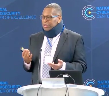
Carl McCants, Special Assistant to DARPA Director, presented the opening keynote on DARPA’s history in the semiconductor supply chain trust and assurance standards. It has been focused on addressing supply chain issues. We had a grand challenge in 2005, where we wanted autonomous cars. We had failed back then.
DARPA has been creating breakthrough, paradigm-shifting solutions. We are accepting and managing risks as well. Concern with globalized microelectronics ecosystem has also been addressed within DoD since 2000. DARPA TRUST and IRIS programs developed the techniques for validating design and process integration before distribution.
He also talked about EDA and testing, and whether the tools were doing what they were expected to do. For IRIS, we focused on what’s happening to the manufacturing process. DARPA SHIELD will develop the facility to provide 100 percent assurance against certain known threat modes quickly, and at any step of the supply chain.
Semiconductor manufacturing supply chain needs to address trust and assurance challenges. We need to maintain the confidentiality of the technology delivered, protect the IP, and have continuous and sustained access to technology needed. We have challenges such as data and definitions, so that a semiconductor product can be delivered without compromise to the product’s integrity, trustworthiness, and authenticity.
For IP protection, we need to incorporate, verify, and validate an IP into design. We need to protect the logic design and simulation of the chip. We also need to be able to transmit and store the functional test programs to the wafer fab facility, and the assembly, packaging, and testing facility. We also have to do aggregation of package-level test data in the APT facility, and take that to the customer.
Model and simulate semiconductor supply chain
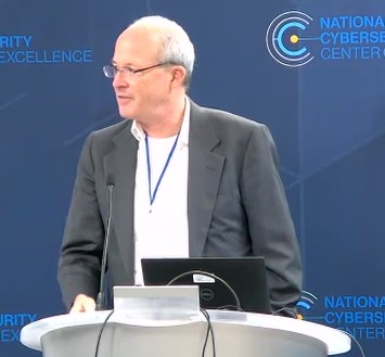
Eric Forsythe, Technical Director, CHIPS R&D, introduced the CHIPS Manufacturing USA. The grand challenge is to seamlessly model and simulate the entire semiconductor supply chain. We need to create an effective collaboration environment for applied industry research to bridge the gap from discovery to production.
CHIPS Manufacturing USA Institute is meeting the digital twin institute objectives. These are: reduce time and cost for chip development and manufacturing, accelerate adoption of semiconductor manufacturing initiatives, etc.
Data — reliable, secure and accessible, workforce development, and model development and validation, were the top three areas to look at. These are the big challenges for developing digital twin technologies for semiconductor manufacturing.
Electronics supply chain digital security standardization
There was a panel discussion on landscape, scope, and focus of electronics supply chain digital security standardization efforts. The participants were Gretchen Greene, NIST, Chris Ritter, Idaho National Lab, and Christophe Bégué, PDF Solutions.
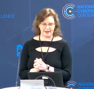
Gretchen Greene, Group Leader, Data Science Group, NIST, said we are currently building trusted chip environments (TCE). We are modernizing the ecosystem and leveraging digital technology. Security and interoperability remain the main issues.
In the CHIPS supply value chain, there are design, fabrication, package, assembly, and test, and commercial sectors. These are addressed by players in muti-physics and modelling, IP, Open Source, manufacturing process and tooling, materials and resources, photonics, microelectronics, etc.
Granularity of the semiconductor supply chain is at the heart of the standards challenge. The interoperability at scale supporting coarse grain digital assets has been inconsistent, and even non-existent. We have the opportunity to impact the industry. We are opening several windows of commercial opportunity for marketplace innovation.
We are also standardizing protocols, such as information sharing, smart connections, etc. We are making protocol specs, payload types, synchronization or process flows, status, managing authorities, verification/validation and resolver services, and registry/curation for monitoring, nodes/hubs, etc.
We are also developing a knowledge network via CHIPS exchange. Semiconductor knowledge can be shared across digital assets, such as taxonomy, machine, actionable, analytics, visualization, etc.
We have goals such as federate across supply chain through use of digital architecture connecting generations, standards, TREs and stakeholders. Strengthen exchange, reuse, and interoperability. Enable discovery and access, etc.
Digital engineering mission
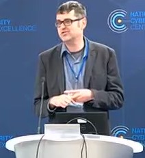
Chris Ritter, Idaho National Lab, said that we have the digital engineering mission. Digital engineering transforms the way we design and operate energy assets. Digital engineering is an innovator and key success driver across all initiatives. It is a key enabler for net-zero program.
With DE, we can design — it links facility information. Operations enable the digital twin. He talked about Deep Lynx, its virtual, and physical platforms. Deep Lynx open source model is a centralized digital twin data warehouse and live event system. Ontological and time series storage of digital twin data streams is there. Event system can push and pull data in real-time around a digital twin. It is proven in operation of MAGNET digital twin.
Idaho National Lab has open ontology for thread and twins. General entity model (GEM) is an extensible, upper-level ontology. It has an advanced manufacturing app. It has digital twin demonstrations across lifecycle stages.

Supply chain traceability
Christophe Bégué, PDF Solutions, said the semiconductor market is currently looking at reliability, RMA or failures in the field, security, and regulation.
Supply chain traceability can provide fast and precise analysis of a reliability or security issue. We can enable short- and long-term containment plans to reduce cost and preserve brand. We can have assurance and preferred supply through provenance and traceability.
We need standards for single device traceability. We have SEMI E142 standard that defines a data model for devices within a wafer or complex assembly. Devices have a virtual identifier (VID) based on this model. E142 forms basis for single device tracking.
We need standards for supply chain traceability. SEMI is developing Specification for Supply Chain Traceability using Distributed Ledger Technology standard proposal to record chain of custody and provenance. We also have SEMI Supply Chain Traceability using distributed ledger technology or DLT. Standard currently defines the data and transaction model, asset lifecycle, and services.
Gina Raimondo updates on US CHIPS Act implementation; Investing in leading-edge technology
Gina M. Raimondo, Secretary of Commerce, USA, gave a speech today at the Center for Strategic and International Studies (CSIS), Washington, DC, on the critical progress CHIPS for America has made over the last year.
Earlier this month, leaders from Departments of Commerce, Defense, and Energy; and the National Science Foundation, and CEO of the National Center for the Advancement of Semiconductor Technology (NATCAST) gathered at the White House to announce over $5 billion in expected investment in the CHIPS R&D program. This includes the National Semiconductor Technology Center (NSTC), and formally establish a public-private consortium for the NSTC.
The announcement included hundreds of millions of dollars of expected investment in the semiconductor workforce, along with the specific funding announcements in packaging, metrology, and a CHIPS Manufacturing USA Institute. This announcement is a reflection of President Joe Biden’s commitment to American innovation and R&D.
Gina Raimondo recalled the space war from the 1960s. CHIPS initiative mirrors the space race that the US had with the Soviet Union decades ago. At that time, President Kennedy issued a call to America to put a man on the moon. Six decades later, President Joe Biden has called for producing semiconductors in the USA, against geopolitics. We can once again cement our leadership role the in global semiconductor industry race.

Raimondo stated that there’s been a game-changer in the demand for leading-edge semiconductor chips. You all know what it is: AI. When we started this initiative in Aug. 2022, generative AI wasn’t even really part of our vocabulary. Now it’s everywhere! Today, AI will become the defining technology of our generation. You can’t lead in AI if you don’t lead in making leading-edge chips. Our work in implementing the CHIPS Act just got a whole lot more important.
US currently leads in design of chips, AI LLMs, etc. But, we don’t manufacture or package any leading-edge chips needed to fuel AI and our whole innovation ecosystem, including chips necessary for national defense. In reality, we were not manufacturing chips in America! We now need to change this, make leading edge and mature chips in America. We need to have lot more semiconductors in America.
The brutal fact is the United States cannot lead the world as a technology and innovation leader on such a shaky foundation. We need to make these chips in America. We need more talent development in America. We need more R&D in America, and just a lot more manufacturing at scale. China is taking an increasing role in their chip production. We have to now nail this! Every detail matters! China is taking an increasingly ambitious role in increasing their own chip production.
We have to nail the implementation of the CHIPS and Science Act. We have to execute like every detail matters because it does and we have to be bold enough with our vision, which is why I liken it to the space race.
We will be judged on two things. First, whether we were able to build a reliable and resilient semiconductor industry that advances our country’s technological leadership. Second, whether we were good stewards of taxpayer dollars. A year into it, I’m proud to say that we are on track to accomplish both. In record time, this team at the Commerce Department has stood up a program, a team, which is flexible, fast, and world class. Over 200 people work in the CHIPS office today. They have a track record of delivering on big projects.
Since President Biden signed the CHIPS Act, and before we put a single dollar out into any private companies, the private sector in USA announced $200 billion in semiconductor manufacturing investments. That’s incredible, and I want to thank the industry.
Nine states have now created new economic development programs. Over 50 community colleges across 19 states have announced programs to partner with the semiconductor industry and opportunities. We are working with the labor unions, academia, research agencies, NSTC, etc., on training workforce for future. NSTC will tackle the R&D challenges facing America’s chips manufacturing ecosystem and upskill, so that we have a skilled workforce.
Focus on targeted investments
We also have some bad news! We have, so far, received over 600 statements of interest, and many of them by strong companies. A significant majority of companies expressing interest aren’t going to receive funding,, including many excellent proposals by strong and worthy companies. Our job is to make targeted investments in relentless pursuit of achieving our national security objectives. We cannot have projects starting in 2030. We need them now.
At the outset, we said that we would invest about $28 billion of the program’s $39 billion in incentives for leading-edge chip manufacturing. The leading-edge companies alone have requested more than $70 billion. We are obsessed with the protection of taxpayers money. We are also going to create thousands of jobs. Companies are also having to go with the national guardrails for these various projects.
We have also made a few decisions. We have decided to prioritize projects that will be operational by 2030. There are many worthy proposals that we have received with plans to come online after 2030. We are saying no, for now, to those projects because we want to maximize our impact in this decade. It’s not responsible to give money to a project that will come online 10 or 12 years from now, if it means saying no to excellent projects that could come online this year.
CEOs generally come in, and ask for billions of dollars. Later, they get half of what they had asked. We have finite amount of money to manage the economy. We have some goals for 2030. Some projects are going to come online in 2030 and beyond. We are not giving the funding for such projects currently. There is risk involved. But, there is way more risk by doing nothing! We cannot be reliant of one part of the world for the most important piece of hardware, and that’s way more riskier in doing nothing!
Two new clusters
Raimondo noted the CHIPS Act goal is to have at least two new large-scale clusters of leading-edge logic fabs, with each of those clusters employing thousands of workers. We expect to exceed that target. We think our investments in leading-edge logic chips will put USA on track to produce roughly 20 percent of the world’s leading-edge logic chips by the end of the decade.
By the end of the decade we are going to go from 0 to 20 percent of leading-edge chips built in the USA. Supply chains will also come along. They can no longer be as vulnerable to geopolitical challenges as they are today. We will also be successful in having leading-edge memory, a critical input for AI systems, right here in the USA.
United States can become the home to the entire silicon supply chain for production of leading-edge chips – from polysilicon production, to wafer manufacturing, fabrication, and advanced packaging. That’s the game, by the way! Let’s be bold! This is not to build a few new fabs, and call it a day. Polysilicon to advanced packaging, and everything in between, including R&D, will happen in the United States.
We are not losing sight of the importance of current generation and mature node chips, which are essential for cars, medical devices, defense systems, and critical infrastructure. Just think back to to the pandemic. We were furloughing tens of thousands of workers from car companies for lack of a single legacy chip. We have got to improve the fragility of that supply chain. We made three announcements of investments in current and mature chip companies – BAE, Microchip, and Global Foundries. We are going to continue to announce additional investments in current and mature production to make sure we have a domestic supply of these critical chips. We are also going to make continuous announcements for materials.
By 2030, the USA will be the only country in the world where new chip architectures can be invented in our new research labs, including those funded by NSTC. They will also be designed in the USA for every end-use application you can think of. Manufactured at scale in the USA by well-paid American workers. And, packaged with the most advanced technology in the world. All on our shores.
Engineering schools all over the country will be pumping out more engineers and technicians trained specifically for the chips industry. We are going to make building hardware sexy again. Today, CEOs are excited. Labor unions are excited. Community college(s) are excited. High schools are excited. They want to know, what can we do to be part of our efforts to revitalize America’s chip ecosystem.
Following the CHIPS Act and other announcements, now, companies are saying: in what state should we expand? With which college should we partner? Where should NSTC be located, and with whom should they partner? We are going as fast as we can. We are more intent on getting this right, and build an industrial base, and beyond. I am excited for what’s going to come.
Implementing CHIPS Act
Earlier, Sujai Shivakumar, Director and Senior Fellow, Renewing American Innovation Project, welcomed the audience. He said that innovation is the engine that powers our nation’s economic growth, competitiveness, and national security. Semiconductors are the platform on which our economy runs, and, on which, so much of our innovation is built. That’s why implementing CHIPS and Science Act is so important.
In various ways, CHIPS pushing the renewable, or how can we manufacture in the United States, greener workforce, connect Americans to the innovation economy, reinvest in our R&D infrastructure, build new public-private partnerships, and cooperate with allies and strategic partners. Importantly, rewire and grow resilient supply chains. All this is to secure the future of US leadership in the 21st century. Semiconductors run everything, We have the CHIPS Act to forward the industry and secure the US leadership in the 21st century.
Fireside chat
Charles Wessner, Senior Adviser (Non-Resident), Renewing American Innovation Project, was engaged in a fireside chat with the Secretary. He asked whether the funding is sufficient to meet the goals. Riamondo stated companies are coming forward, and setting up the ecosystem. This is achievable with the money that we have.

Next, TSMC has spent about $30 billion in expansion. National Fund in China spent about $41 billion. Where does USA stand? Raimondo said China is not exactly shy about their ambitions. They have also poured $100 billion in domestic chip production. Leading-edge chip producers in the USA are majorly American, such as AMD, Intel, Nvidia, Microsoft, etc. What TSMC is doing in Arizona is path breaking. They are investing in United States. We are grateful for that, and are going to make sure it’s successful.
Legislation requires that we also invest $2 billion in foundational chips. GlobalFoundries is doing foundational chips and that alone was $1.5 billion. We are going to exceed the $2 billion mark. We can easily invest a bit more in the excellent companies. We can now do leading-edge chips, leading-edge memory, and and current mature, and still have some for the supply chain.. We are also keeping the tax credits. Tax credits will be shown to have been an unbelievably powerful part of the incentive to stretch the capital. That is why we’re able to do so much with relatively limited grant money.
We also envision the NSTC and NATCAST to be some part of R&D, and also launching workforce centers of excellence as the national hub for semiconductor training and excellence. We are also developing the semiconductor curriculum. We hope this can go ahead and unify the industry. Companies also want to make sure that the talent supply is available here in USA. That will be an important work for the NSTC.
We are now meeting the moment with leading-edge semiconductors, and meet the needs of AI and other technologies. We need to succeed! Failure is not an option here!! Imagine, if we are dependent on a couple of countries in Asia for such chips!!! We now need to lead the world in this kind of advanced technology. America is a world leader, and we intend to remain that way. We also need to keep up with the talent.
The President’s called many times for responsible immigration. We need to keep that talent. I would be strongly supportive of something that maintains highly skilled immigrants for this industry. It doesn’t have to be so narrow. I wish it were broader than just the chips industry. But, it’s a huge thing that does keep me up at night.
Wessner added that the space race is a good metaphor. Every decision is difficult and it helps us to have a dialog, noted Raimondo. We have spoken with several Governers, and other Senators. They have been strongly supportive of the CHIPS Act. They also want more jobs in their states, We have limited money right now, and there will be tough choices initially.
Wessner stated that NSTC seems to have enough potential. How do you see its longevity? Raimondo said NSTC has to be built for the decades to come. We have announced the Board and Woman to run that. We will also have workforce centers of excellence. We have to maximize on this.
Lastly, what will happen to the smaller companies? Is anything being done for them? Raimondo said we are determined to give small grants to small companies. There are many innovative companies in the semiconductor supply chain. They are not building big fabs. They might have materials that are innovative or somehow, provide inputs to fabs. We have a whole initiative internally to look at small companies to give them small grants. The majority will be told no, but many small companies are going to get funded.
NSTC will set up infrastructure, whether labs or testing facilities or prototyping facilities, digital twin facilities for little companies to use, and to have access to equipment and talent that they otherwise couldn’t afford. She does not know what the next wave of innovation is as these chips get smaller. Small companies should have access to labs and facilities so they can develop new technology, even though they’re capital constrained.
Update on CHIPS Act implementation, and recommendations from IAC Working Groups
Industrial Advisory Committee (IAC), Chips.Gov, USA, organized a conference today.
Mike Splinter, Chair, IAC, said, the IAC has approved several recommendations since inception. Many are also works in progress. There are areas that further need work, such as NSTC, development of standards, etc. He thanked members for their dedication toward IAC. Commerce will be announcing new members very soon.
Susan Feindt, Vice Chair, IAC, added that key issues and challenges are being addressed. We are looking forward to hearing new recommendations. She thanked the DoC, Chips R&D Office, etc., for their work, as well as the IAC members. She welcomed the NSTC members of the incoming board of trustees. They include Robin Abrams, Craig R. Barrett, L. Reginald Brothers, Nicholas Donofrio, Donna L. Dubinsky, Erica R.H. Fuchs, and James D. Plummer.

Laurie E. Locasio, Director of NIST and the Under Secretary of Commerce for Standards and Technology, stated her thanks for the audience’s interest in Chips Act. We celebrated the one-year anniversary of the Chips Act a few months ago. New communities are now coming in. We have several opportunities for the Chips Act workforce community.
Chips for America will also go hand-in-hand with manufacturing, and R&D. It will also drive education and workforce development, etc. We are very excited of the opportunities that will be provided in future. Regarding the NSTC, she welcomed the new board of trustees. Later, we will announce the establishment with a new non-profit. Indeed! SemiUS, a new non-profit entity, was announced as future operator of the National Semiconductor Technology Center (NSTC) on Nov. 8, 2023.

Lora Weiss, Director, Chips R&D Office, NIST, introduced her team. They include Eric Lin, Richard-Duane Chambers, Maria Dowell, Jay Lewis and Subramanian Iyer. Since President Joe Biden set the Chips for America Act, the mission has been accelerating. It is accelerating development and commercial deployment of foundational semiconductor technologies. We also need tools, workforce, etc.
2030 goals include US technological leadership, accelerate ideas to market, and develop a robust semiconductor workforce. Chips R&D programs are integrated with each other. These include metrology, NSTC, NAPMP, and Manufacturing USA Institutes.
Metrology program grand challenges include metrology for materials purity, properties, and provenance. Advanced metrology for future microelectronics manufacturing, modelling and simulating semiconductor devices, materials, and components, etc. We also had a Standards Summit in Sept. 2023. The outcomes include shared goals for the community standards. The report will be coming soon.
Chips for America will also need a workforce program. We need to align semiconductor education, increase awareness of opportunities, and accelerate access to educational resources.
IAC recommendations
Eric Lin, CHIPS R&D Deputy Director, NIST, talked about IAC recommendations. We have now made lot of progress. We have working groups that look at R&D gaps, organization and public-private partnerships, and workforce development. The R&D Group will look at long-term research needs of the industry. Second group will review all funding sources, and map out relationships. Third Group will look at workforce needs of the industry.

We will establish set of five key capabilities aimed to lower the barriers to entry and success for innovators. We will identify app-driven grand challenges to inspire innovation across computing stack. Chips R&D programs must demonstrate relevance via support and contributions from all stakeholders.
For organizational and PPP, working Group recommends that DoC structure NSTC as a public-private consortium. SemiUS will be the new non-profit entity. Subcommittee also recommends fiduciary board for NSTC. It recommends recruiting a highly respected executive to serve as CEO, NSTC.
NSTC should be led by an independent CEO. It should develop a sustainable business model. NSTC should offer prototyping enable-ment along with translation path to domestic volume production sources. It should be a funding mechanism for coalitions of excellence, and for projects executed within and across the coalitions. NSTC should partner with ecosystem.
CEO should have autonomy on how the organization goals are executed. CEO should understand the current in US semiconductor industry leadership. Structure of NSTC must foster healthy competition. There should be Technical advisory board (TAB) assignments and process.
For workforce, we should create a strong coordinated inclusive workforce development and training program. Chips R&D Program Office, with its component R&D programs, should define metrics by which the success of semiconductor and microelectronics workforce development programs are to be measured.
All post-secondary educational institutes receiving funding through R&D programs should be incentivized to participate and contribute to collaborative national network for microelectronics education. National network will be expected to facilitate access to hands-on learning opportunities. The participants should also develop, implement, and assess new pedagogical approaches.
DoC should support coordinated efforts to create excitement and awareness in K-12 students and families. Then-Governer Gina Raimondo had pioneered for comprehensive computer science education in Rhode Island. Experiential microelectronics education for students in grades 9-12 also has the potential to grow the microelectronics workforce pipeline. We are also grateful for the IAC’s recommendations.
CHIPS for America NOFO for supply chain facilities below $300 million
CHIPS for America announced its second notice of funding opportunity (NOFO) to strengthen the USA semiconductor supply chain, advance technology leadership, and support vibrant domestic semiconductor clusters. It is now open to smaller supply chain projects and businesses seeking to construct, expand, and modernize materials or manufacturing equipment facilities with capital investment below $300 million.

US Department of Commerce announced the funding opportunity for smaller supply chain projects and businesses to access CHIPS for America funds. As part of President Biden’s Investing in America agenda, the bipartisan CHIPS and Science Act includes incentives to strengthen supply chains, support smaller projects and businesses, and create good-paying jobs in local communities across the country.
Projects will produce equipment, chemicals, gases, and other materials, critical to manufacturing semiconductors in America. Suppliers are strongly encouraged to apply for CHIPS incentives alongside other institutions from their regions to expand their economic opportunity and competitiveness.
The investments made as part of this new funding opportunity will support three strategic objectives as outlined in our “Vision for Success”:
- Strengthen supply chain resilience,
- Advance US technology leadership; and
- Support vibrant US fab clusters with a reliable ecosystem of suppliers.
Ms. Gina Raimondo, Secretary of Commerce, said, “CHIPS for America is laser-focused on ensuring both our economic and national security by making smart investments up and down semiconductor supply chains that enable smaller suppliers and more American workers to help grow the US semiconductor industry.”
In a seminar, Ms. Jesse Stoneman, Deputy Director, Public Engagement, CHIPS Program Office, said we are sharing our strategic vision for the smaller-scale supply chain projects funding opportunity. The announcement is on $39 billion for the manufacturing program of CHIPS for America Act. It is for the semiconductor materials and equipment facility projects under $300 million.
We had two funding opportunities earlier: first, for commercial leading-edge, current, and mature node fabrication facilities, and second, for large semiconductor materials and equipment facility projects over $300 million. We will have a final opportunity to support the construction of semiconductor R&D facilities. So far, CHIPS Program Office has received over 500 statements of interest, and 100+ pre-applications and full applications.
Ms. Nikita Lalwani, Senior Advisor to Director, CHIPS Program Office, said this funding opportunity has been tailored for smaller businesses. It has priorities such as economic and national security objectives, commercial viability, financial strength, technical feasibility and readiness, and workforce and community investment.
We need to strengthen supply chain resilience, and advance US technology leadership. USA will have incentivized major US equipment and materials suppliers to increase their footprints in the USA. Non-US suppliers of world’s most advanced equipment, materials, and sub-systems will also establish large-scale footprints in the USA.
By the end of this decade, we should be able to support vibrant US fab clusters. Each CHIPS-funded fab cluster in the USA will be supported by dozens of suppliers, including many investing in USA for the first time. State and local entities are encouraged to help facilitate the expansion of these ecosystems.
Ms. Olivia Briffault, Investment Principal, CHIPS Program Office, detailed funding instruments. For total funding, up to $500 million in direct funding is available in total. For funding by projects, direct funding is expected to be 10 percent of project capital expenditures. A ‘lender marketplace’ will connect the loan-seekers with private sector institutions. CPO is also exploring other opportunities to provide credit.
Applications will be accepted between Dec. 1, 2023, and Feb. 1, 2024. For applications that are invited to the full application phase, the program will communicate submission dates individually upon notifying them of their advancement. Concept plans will no longer be accepted on a rolling basis. Unlike previous funding opportunities, no statement of interest is required under this NOFO.
The concept plan submitted should describe how the proposed project addresses the core program priorities. It will be used by the Department to score applicants and invite those most likely to receive an award to advance to the full application phase. The Department will invite the most promising applicants to the second phase, where they will have the opportunity to submit a full application.
Concept plan evaluation criteria includes: Extent to which a project advances USA economic and national security. Project’s long-term commercial viability, including robust customer demand for the proposed project output. CHIPS incentives justification. Likelihood that applicant will successfully execute the project, including construction and environmental review. Availability of non-CHIPS funding sources.
Ms Lalwani added that in the full application, you will be asked to submit a Workforce and Community Investment Plan containing construction and facility workforce strategy, and community investment strategy. Consortium members may collaborate on this plan.
We are also defining consortia and clusters. For consortium, there should be entities working to build vibrant US semiconductor fab clusters. For cluster, look at geographically compact area with multiple commercial scale fabs owned and operated by one or more companies, R&D facilities, specialized infrastructure, such as chemical processing and water treatment facilities, nearby suppliers to the semiconductor industry, diverse, and skilled workforce, etc.
A strong consortium should have at least two suppliers, a state or local government entity, an anchor institution. It may also contain workforce training providers, labor unions, economic development corps, etc. Members may develop one strategy at the consortium level covering each consortium member. Consortia is strongly encouraged for applicants claiming to benefit US clusters. Consortia is welcome for applicants claiming to support the other two objectives.
Consortium participants example includes supplier facility, state or local government, higher education institute, semiconductor fab, economic development corporation, workforce provider, labor union, etc.
This new funding opportunity features an application process designed to be accessible for smaller businesses and projects. The application process includes two phases:
Concept plan: Applicants will be asked to submit a concept plan describing how their proposed project addresses core strategic objectives, including US economic and national security. Concept plans will be accepted between December 1, 2023, and February 1, 2024.
Full application: The Department of Commerce will review submitted concept plans and invite the most promising applicants that demonstrate how they advance program priorities to submit a full application for CHIPS incentives. The full application submission dates will be communicated to applicants individually upon notifying them of their advancement.
FAQs
Some FAQs were raised. One: there is no fab in my area. Can I still make the case that I am advancing a US fab cluster? Yes. The Department is interested in projects that advance clusters by closing critical gaps in the US supplier landscape. Often, projects will accomplish this goal by locating near the fabs to reduce burdens associated with transporting critical supply chain inputs. But, that is not a requirement. The Department welcomes projects that support clusters in other ways, including by providing critical materials or equipment to fabs in multiple areas.
Next, how do I apply as part of a consortium? Each member of a consortium seeking funding for a project eligible for CHIPS Incentives must submit their own separate concept plan and application. As part of the concept plan and application, consortium applicants will be asked to submit a ‘consortium narrative’ detailing other consortium members, and setting forth the overall strategic vision of the consortium, among other relevant information.
Applicants that are part of the same consortium should submit the same information in their consortium narrative.Funding will be awarded on a per-project basis to consortium members proposing to construct, expand, or modernize a facility eligible under the second NOFO. For more information, see Sections I.B.4 (“May applicants apply for funding under this NOFO as part of a consortium, and if so, how?”) and IV.G.2 and IV.H.2 (“Consortium Narrative”) of NOFO 2.
Will the consortium receive funding as a whole? Funding will be awarded on a per-project basis to consortium members proposing to construct, expand, or modernize a facility eligible under NOFO 2. Eligible uses of funds include costs to:
- finance the construction, expansion, or modernization of a facility, or equipment for that facility,
- support site development and modernization for a facility,
- support workforce development for a facility, and
- pay reasonable operating expenses for a facility, as determined by the Department.
What should state and local governments do if they want to form or support a consortium application? State or local government entities that join consortia are strongly encouraged to take steps to build and support vibrant semiconductor clusters. Such steps might include investments in workforce, education, site preparation, research and development, or infrastructure (including transportation, housing, water, or energy) designed to benefit both the consortia members and the broader community.
State and local government entities in consortia are also strongly encouraged to help streamline access to resources critical to cluster growth, such as permitting and expansion services, and coordination with relevant regulatory authorities. For consortia that include a state and/or local government entity, the “consortium narrative” should list any actions that entity is taking or intends to take to facilitate cluster development.
The Department expects that strong consortia will include an anchor institution such as a semiconductor fab. What are other examples of anchor institutions? Besides, semiconductor fabs, the anchor institutions could include large suppliers, universities, and/or advanced packaging facilities. Along with the anchor institutions, strong consortia will also include at least two suppliers, and state or local government entity, and may include entities such as workforce training providers, economic development corporations, labor unions, institutions of higher education, philanthropic foundations, industry organizations, Tech Hubs, or other relevant entities.
Are there downsides to requesting an award of more than 10 percent of project capital expenditures? If an applicant requests more than 10 percent in CHIPS Direct Funding, the Department expects that it may take substantially longer to evaluate the full application and prepare an award. In addition, the applicant will need to make a particularly compelling case that their project advances the Department’s economic and national security objectives. Additional funding is necessary to make the project commercially viable.
CHIPS for America: Final rule preventing improper use of CHIPS Act funding
US Department of Commerce released the final rule today, implementing the national security guardrails of the bipartisan CHIPS and Science Act.
The rule elaborates on two core provisions of the statute. First, prohibiting CHIPS funds recipients from expanding material semiconductor manufacturing capacity in foreign countries of concern for 10 years. Second, restricting recipients from certain joint research or technology licensing efforts with foreign entities of concern.
Chips.gov, USA, organized a conference today on preventing the improper use of CHIPS Act funding. It covered the final rule implementing national security guardrails of the bipartisan CHIPS and Science Act.
This rule seeks to prevent foreign countries of concern from accessing cutting-edge technology that is developed with US funds, while helping to ensure CHIPS investments enhance global supply chain resilience in co-ordination with allies and partners.

Dr. Ms. Morgan Dwyer, Chief Strategy Officer, CHIPS Program Office, said we made two announcements regarding funding opportunities. First was in Feb. 2023, for commercial leading-edge, current, and mature node fabrication facilities. Next was in June 2023, for large semiconductor materials and equipment facility projects worth $300 million+.
Later, we will announce programs for smaller semiconductor materials and equipment facility projects under $300 million, and support for construction of semiconductor R&D facilities. The CHIPS Program Office has received over 500 statements of interest and 100 pre-applications and applications.
On March 21, 2023, the Department had released Notice of Proposed Rulemaking, and began accepting public comments. The 60-day comment period closed May 22, 2023. We received comments from industry, trade associations, labor, and government.
Today, on Sept. 22, 2023, we are releasing the final rule implementing the guardrails. It is for preventing the improper use of CHIPS Act funding. National security guardrails are intended to ensure that funding provided through this program does not directly or indirectly benefit the foreign countries of concern. Strong national security guardrails will help protect the national security of America, and its partners and allies. We will continue coordinating with allies and partners to ensure these guardrails advance shared goals, strengthen global supply chains, and enhance our collective security.
The final rule addresses two separate guardrails from the CHIPS Act: Expansion guardrail and Technology guardrail. Both guardrails permit the Department to recover the entire award, if violated. The final rule details how both guardrails will work, and the process for evaluating and mitigating possible violations.
Key guardrails
Vikram Vishwanathan, Director of Policy, CHIPS Program Office, US Department of Commerce, stated that the final rule establishes the scope of restrictions on expansion of semiconductor manufacturing capacity in foreign countries of concern. It defines the scope of exceptions, including for facilities producing legacy semiconductors. These come under the expansion guardrail.
Under technology guardrail, the final rule details restrictions on joint research and technology licensing efforts. It also details additional conditions to prevent circumvention of the technology claw back by entities related to the funding recipient.
We appreciate the detailed comments received, including from government entities, industry associations, and multinational semiconductor companies. We have made several significant changes in response to those thoughtful comments.
The final rule ties the expansion of semiconductor manufacturing capacity to the addition of cleanroom space, which allows for equipment upgrades and efficiency improvements within the existing space. The final rule includes several exceptions for the joint research and technology licensing claw back that are not a threat to national security, such as certain pre-existing activities, activities related to international standards, and those involving patent licensing. Final rule includes semiconductor wafer manufacturing within the definition of semiconductor manufacturing.

Expansion guardrail overview
Presenting the Expansion Guardrail final rule overview, he said companies receiving CHIPS funding, as well as members of their affiliated group, may not build new facilities or expand existing facilities in foreign countries of concern for 10 years.
To allow existing facilities to continue ordinary operations (such as tool upgrades and replacements), they may upgrade manufacturing capacity by 5 percent. Existing facilities manufacturing legacy semiconductors are excepted. However, they may not increase capacity by 10 percent or more.
The existing facilities may upgrade their technology, but export controls may still apply. Exception for new legacy facilities that predominantly serve the country of concern requires that 85 percent of the final products containing the chips be used or consumed in that country.
A covered entity and its affiliated group may not engage in any significant transaction involving the material expansion of semiconductor manufacturing capacity in a foreign country of concern for 10 years following an award. Violations of prohibition may trigger full claw back of the CHIPS award.
Exceptions include existing facilities for producing legacy semiconductors, and facilities for producing legacy semiconductors that predominantly serve the domestic market of the foreign country of concern. Foreign countries of concern include China, Russia, North Korea, and Iran. Secretary of Commerce, Ms. Gina Raimondo, may add other countries, if required. The CHIPS Act defines affiliated group to generally mean an entity that has 80 percent common ownership with the covered entity.
In the final expansion guardrail rule, significant transaction will be defined in each individual award agreement. Material expansion means an increase in semiconductor manufacturing capacity by more than 5 percent via addition of cleanroom, production line, or other physical space. Semiconductor manufacturing capacity includes wafer production, semiconductor fabrication, or packaging.
Existing facilities means a facility that was built, equipped, and operating prior to award or, at the Secretary’s discretion, a facility being equipped or expanded at the time of award. A facility that has undergone a significant renovation increasing capacity by 10 percent or more is no longer an existing facility.
In legacy semiconductors, for logic, 28nm or older (from statute). For DRAM, half pitch 18nm. For NAND, <128 layers. However, this does not include any semiconductor packaged with 3D integration, post FinFET chip, or semiconductor critical to national security. Lastly, it predominantly serves the market. At least 85 percent of a facility’s output is incorporated into final products that are used or consumed within the market.
Technology guardrail overview
Under technology guardrail, companies may not generally engage in joint research or technology licensing related to technology or products that the Secretary has determined raise national security concerns (i.e., certain export controlled semiconductors or semiconductors critical to national security) with foreign entities of concern.
The final rule articulates those categories of technology or products that raise national security concerns. Technology Guardrail does not apply to joint research or technology licensing that was ongoing prior to the issuance of the final rule. Such ‘grandfathered’ activities must be memorialized in the agreement between the covered entity and the Department. The final rule includes additional conditions to prevent circumvention of the technology.
A covered entity may not knowingly engage in any joint research or technology licensing effort with a foreign entity of concern that relates to a technology or product that raises national security concerns. This prohibition does not apply to joint research or technology licensing that was ongoing prior to the issuance of the final rule. Violations of this prohibition will result in the mandatory recovery of the entire CHIPS award.
In the final technology guardrail rule, the applicable term is defined in each award agreement. For joint research, it is any R&D jointly undertaken by two or more people, including the R&D undertaken as part of a joint venture. It exempts five categories, including standards work, engineering related to using a foundry, and warranty services.
In technology licensing, there can be be an agreement to make trade secrets or know how available to another party. It exempts the same categories above, as well as patent licensing. As for foreign entity of concern, it includes entities on sanctions lists and adds BIS’s Entity List and Treasury’s Chinese Military Industrial Complex Companies (NS CMIC) list. The term includes companies organized or with a principal place of business in a foreign country of concern, as well as individuals resident in those countries.
In technology or product that raises national security concerns, any semiconductor critical to national security or electronics, which are export controlled for national security or regional stability reasons (including items controlled as part of the October 7 rules).
Finally, semiconductor critical to national security includes chips used for quantum computing, in radiation intensive environments, and for other specialized military capabilities. The list was developed with input from DoD and the IC.
There are additional conditions on certain joint research or technology licensing. Technology guardrail applies only to the covered entity and, if triggered, results in the mandatory recovery of the entire award. To prevent circumvention of the technology guardrail, the final rule establishes that the Secretary may take appropriate remedial measures, where any related entity of a covered entity engages in joint research or technology licensing that would violate the technology guardrail, if engaged in by the covered entity.
A related entity is any entity that directly, or indirectly through one or more intermediaries, controls or is controlled by, or is under common control with, the covered entity. Appropriate remedial measures, include requiring a mitigation agreement, partial recovery of an award, and full recovery of an award.
Department of Commerce has appreciated input from partners and allies, while developing the
guardrails. We will continue coordinating with allies and partners to support a healthy global semiconductor ecosystem that drives innovation and is resilient to cybersecurity threats, natural disasters, pandemics, geopolitical conflict, and more.
As semiconductors and technologies continue to evolve, the US will work with allies and partners to ensure the latest technology cannot be used by malign actors to undermine our collective economic and national security. We will continue coordinating closely with US partners and allies to advance these shared goals, advance our collective security, and strengthen global supply chains.
In brief, the final rules:
- Prohibits recipients of CHIPS incentives funds from using the funds to construct, modify, or improve a semiconductor facility outside of the United States;
- Restricts recipients of CHIPS incentives funds from investing in most semiconductor manufacturing in foreign countries of concern for 10 years after the date of award; and,
- Limits recipients of CHIPS incentives funds from engaging in certain joint research or technology licensing efforts with a foreign entity of concern that relates to a technology or product that raises national security concerns.
If these guardrails are violated, the Department of Commerce can claw back the entire federal financial assistance award.
So, how will this affect companies having existing operations in foreign countries of concern? Will they still be able to apply? CHIPS Program Office strongly encourages applications from companies outside the United States. Companies with existing operations in foreign countries of concern may apply for and receive CHIPS funding.
All funding recipients will be subject to our guardrails to protect national security. The guardrails were designed to prevent future investment in countries of concern, and to allow existing facilities to continue viably operating to avoid disrupting existing supply chains, consistent with any applicable US export control regulations.
Do the guardrails require CHIPS funding recipients to cease manufacturing in the foreign countries of concern? The answer is NO, with some exceptions, the guardrails will not affect the existing operations of CHIPS funding recipients in foreign countries of concern.
The rule allows for these facilities to continue operations and undergo reasonable upgrades consistent with any applicable US export control regulations. The guardrails are focused on the expansion of semiconductor manufacturing capacity and joint research or technology efforts related to technology and products that raise national security concerns. The guardrails do not generally regulate all technology.
Personally, I just wish, something like this was done in India!
