
Bridging digital and physical worlds with efficiency and intelligence!
2024 IEEE Symposium on VLSI Technology & Circuits will be held June 16-20 at the Hilton Hawaii Village, Honolulu, Hawaii. The conference theme is bridging the digital and physical worlds with efficiency and intelligence.
Gosia Jurczak, Lam Research, and Borivoje Nikolić, University of California, Berkeley, are the Symposium Chairs. Takaaki Tsunomura, Tokyo Electron Ltd and Mototsugu Hamada, The University of Tokyo, are the Symposium Co-Chairs.
Vijay Narayanan, IBM T. J. Watson Research Center, and Ron Kapusta, Analog Devices, are the Program Chairs. Kazuhiko Endo, Tohoku University and Sugako Otani, Renesas Electronics Corp., are the Co-Chairs.

The plenary speakers are: Dr. Ahmad Bahai, CTO, Texas Instruments, on making sense at the edge. Dr. Maryam Rofougaran, CEO, Founder, Movandi Corp., on wireless and future hyperconnected world. Hidehiro Tsukano, Senior VP of R&D, NTT Corp., on photonics-electronics convergence devices to accelerate IOWN. Dr. Kazuoki Matsugatani, Senior Director, R&D Center DENSO Corp., on mobility evolution: electrification and automation.
The conference commences June 16 with standing workshop and three parallel workshops. The standing workshop is on advancing SoC design: open-source and ML-driven approaches in the cloud. Three parallel workshops are: novel metals for advanced interconnect, high-performance mixed-signal circuits: recent art balancing the analog vs. digital effort, and biosensory breakthroughs: pioneering the future of health tech.
June 17 has short courses on tech and circuit each, and a demo session. Circuit course is on circuits and systems for heterogeneous integration. Tech course is on advanced VLSI technologies for next-generation computing. Demo session, first introduced in 2017, has 15-20 demos.
June 18 has plenary talks, regular paper sessions, WIC and YP event, and an evening panel discussion. Joint panel for circuits and technology is on: Will AI bite the industry that feeds it? It will be moderated by Tokyo Institute of Technology. There will be seven participants from Qualcomm, KLA, SK Hynix, imec, Nvidia, KAIST, and Stanford University. There will be a game-show like competition between chip heroes (panelists and audience) and gen-AI.

There will also be Women in Circuits & Young Professional Mentoring event, Test of Time award, VLSI Symposia Best Student Paper award (BSPA), with a winner each for circuits technology, and Best Demo Paper award. June 19 has plenary talks and regular paper sessions.
June 20 has regular paper sessions and luncheon talk. Luncheon talk will be on CHIPS Program and you: an R&D update for VLSI symposia. It will be delivered by Greg Yeric, Director of Research, CHIPS National Semiconductor Technology Center Program, CHIPS R&D Office, US Department of Commerce.
There are 17 technology sessions, such as oxide semiconductor applications in BEOL, backside of silicon: from power delivery to signaling, NVM — Hafnia-based ferroelectrics-1, novel channel materials for advanced CMOS, etc.
There are 29 circuits regular sessions, such as wireline circuits, power at high voltage and current, AI/ML accelerators and CiM, biomedical stimulation and imaging, etc.
There are six joint focus sessions, such as RF, mmWave, and THz technologies, processors and compute, thermal management and power delivery in 3D integration, biomedical technologies, image sensors, and memory-centric computing for LLM.
VLSI 2024 will see historical high for paper submissions, totaling 907. 41 percent of the accepted papers are from the industry. The USA and Korea have the highest number of accepted papers, followed by China and Taiwan. Other countries include Japan, Belgium, Singapore, France, Switzerland, etc.
Global semiconductor industry forecast updated to +4.9 percent to $552.762 billion for 2024: Future Horizons
IFS 2024 semiconductor industry mid-year outlook by Future Horizons, was held today in Kent, UK.
Malcolm Penn, Chairman and CEO, started with the really good news first. Downturn had bottomed in Q1-2023. Golden cross was breached in July 2023. Then, the really worrying news! It was supposed to be sunshine. Suddenly, there’s storms on the horizon. The death cross could hit as early as June or July 2024. Let’s hope (and pray), this proves the fallacy of extrapolations.

The 2023 market took off with a vengeance. It bottomed out at $119.511 billion at -8.2 percent in Q-23. In Q2-23, there was strong rebound at $126.714 billion at 6 percent. In Q-23, there was solid growth at $134.674 billion at 6.3 percent. Q4 saw above seasonal growth at $145.986 billion at 8.4 percent. 2023 finished at $526.885 billion, with -8.1 percent growth.
Downturn bottomed one quarter earlier than the ‘4-quarter norm’. Ultra strong Q2 was an unexpected surprise, even to TSMC. Q3 powered forward at strong seasonal level, and Q4 was even stronger. Semiconductor industry was originally forecast at -8 percent vs. -20 percent in 2023. ‘Super cycle’ (irrational) exuberance pitched 2025 forecasts in the ‘high 20 percent’. So, what could possibly go wrong?
The wheels fell off in Q1-2024. The global semiconductor industry moved from +8.4 percent to -5.7 percent in Q1-24 to $137.717 billion. Was this train wreck or fender bender? Whoever said this industry can’t still pull surprises?
Monthly IC growth rate turned steeply positive in Sep. 2023, and then, plateaued in Dec. Opto and discretes were still deeply in recession. Was it more representative?
There are four sides to the same cycle. All IC sectors follow the same cyclical pattern. No sector is immune. Logic first (Jun. 2023), and then micro (Jul. 2023), followed by memory (Sep. 2023). Analog ICs still have yet to recover (Mar. 2024?).
Europe has finally succumbed to the semiconductor recession. Having weathered the downturn, Europe has now fallen on its sword. Weak economy and heavy dependence on automotive and industrial are said to be factors. Is this more indicative of underlying global market health?
Looking at the global IC annual growth rate unit and value trends, recovery in market value was driven by Q2-2023 IC ASP rebound. IC unit growth has yet to recover. Also, watch out for IC ASP growth rates that may crash mid-2024.
Downturn recovery was: units first, and ASPs a year later. But, not this time, as it was ASPs first, and in 40 years history, it’s never happened before! This flies in the face of free market economics supply/demand fundamentals. It may either be a quirk of math (percentages can be misleading).
Take a hard look at the details! Strong market value growth was driven by ASPs, and not units. We make and sell units, not dollar bills. We have still ongoing excess inventory and slow end-market demand are underlying causes for lackluster demand. Current situation is exacerbated by hangover impact of plethora of long-term price agreements (LTAs) from post-Covid-19 market boom.
This is aided and abetted by slowdown in demand due to impact of inflation and interest rate rises on consumer and business spending. Capacity utilization rates are mostly in 70-75 percent range. The bulk of chip market is not Nvidia GPUs and AI apps. It is hard to call a recovery, when the unit demand is in doldrums. 2023 was never the start of another semiconductor super-cycle!
Industry outlook
The global economy is still shrouded in confusion and uncertainty. We are trapped in a roller-coaster netherworld of divergent economic reports. Rise in US labor costs sent two-year treasuries yields over 5 percent. It was counteracted three days later by report of smallest increase in wages since 2021.
US retail sales are seemingly surging, yet GDP growth is slowing. Industrial production has been rising, while manufacturing has been easing. Jobless claims are holding steady, yet, hiring has ticked down. There is will they or won’t they conundrum on high interest rates and inflation. If you feel confused, it is rightly so! And, so, too is the market!
US unemployed job seeker rates have hit parity. Arizona and New York state are set to soon join this list. One or more ratio is bad news for job seekers, but good for economy. The trend is in line with the Fed’s gradual labor market cooling agenda.
Eurozone finally exited recession in Apr. 2024. Q1-2024 GDP increased 0.3 percent vs. Q4-2023. This is the strongest pace in 18 months! Consumer prices rose at an annual 2.4 percent rate in March and April. June is now seen as the ECB’s likely start of EU monetary easing.
The stock market has remained remarkably calm. Semiconductor market needs a strong economy to thrive. When interest rates rise, cost of borrowing goes up. This impacts the cost of cars, credit cards, and mortgages. Impact is cushioned by high post-Covid-19 savings and credit card borrowings. These are not a bottomless pit! One day spending cutbacks are inevitable.
Unit shipments are still way below long-term average. It is currently 24.6 percent below 8.2b/week maxed out peak, and 14.1 percent below long-term trend line. 69b units are still to go! It is highly improbable that the much-vaunted unit balance will happen this year. We can’t claim recovery until IC unit growth resumes!
Capex is finally cutting back. Capex percent IC sales peaked Q1-2023 at highest rate ever, beating Dot.Com bubble boom. Feb. 2024 saw total spend back to the 14 percent safe-haven level. Capex cutback is likely for rest of 2024, given soft unit demand (tech Pull vs. capacity build). Also, global new fab capacity starting production in 2024 is up 6.4 percent (42) vs. 2023 (11).
China impact
There is the impact of China on capex. Non-China capex cut back started on cue in Q2-2023, or, three quarters after market collapse. China spend has now reached an apocalyptic proportions of 47.2 percent of total capex spend. Current level is 34 percent higher than 2023, and 80 percent higher than 2022. China capex is a serious red flag, aka solar panels, EV batteries, and vehicles.
As per TrendForce, China chip production should rise 60 percent in next two years, and be 2X in five years. New units are now completed or under construction, or planned in places, such as Beijing, Tianjin, Jilin, Dalian, Qingdao, Yancheng, Wuxi, Suzhou, Shanghai, Hangzhou, Chengdu, Wuhan, Xi’an, Hefei, Nanjing, Xinxiang, etc.
ASPs are moving from rout to recovery. IC ASPs peaked in Feb. 2024, and 52 percent higher than July 2022’s $1.10 downturn low. We can expect to see an ASP correction in H2-2024, especially given the industry overcapacity. What goes up (down) must go down (up), with long-term average growth is zero.
Market forecast
So far, economy is an enigmatic mix of contradictory factors. Unit demand is running way below long-term average. In capacity, non-China capex has now prudently reined back. We have massive China overspend way beyond needs. ASPs have been in steep upward trajectory since May 2023.
There is red flag alert – chip market fundamentals are still systemically very weak. We have continuing unsettled economic and geo-political outlook. Longer-term potential pressure is on mature market nodes, thanks to China, plus Chips Acts.
Forecast revised to +4.9 percent
In Jan. 2024, we forecast the global semiconductor industry to be +16 percent, an upward revision from Sept. 2022 9 percent. 17th industry up cycle started in Q1-2023, and ASP is not unit driven. 2024 forecast is now +16 percent (+12 percent bear and +20 percent bull. Enjoy the value growth spurt, but, beware ‘spreadsheet’ vs ‘real recovery’. Worsening economic outlook can push recovery into bear territory.
Q1-2024 crashed, and +3 percent forecast became -5.7 percent actual, down from Q4’s 8.4 percent. Market crash was sudden and unexpected, starting in Jan. 2024. IC unit demand started to fall through the floor. At the same time, IC ASP growth stalled. The combined impact was calamitous, wiping $10 billion from the forecast. Negative Q1 now makes Q2 growth unlikely. Now, more than ever, keep a strong eye on the data.
There is no way now that 2024 will be double-digit growth. We are back to the drawing board for our 16 percent forecast for global semiconductor industry in 2024. We have now updated forecast for 2024 to +4.9 percent to $552.762 billion. $56 billion were wiped off the new full year number. We are back to Sept. 2023 single-digit number. We are back to 2021’s $555 billion number! Bullish forecast is 8 percent growth to $569.086 billion for 2024.
Key takeaways
The notion that AI will take over the world is pure science fiction. They do increasingly more complex grunt work! But, unlike humans, they can’t do things such as imagination, originality, kindness, creativity, gut feeling, joy, sadness, ecstasy, pride, depression, love, feeling of ownership, physical pleasure, physical pain, mental turmoil, etc.
In automotive, all roads lead to China. An increasing number of MNCs seemingly believe the only way to catch up with Chinese carmakers, which have prioritized EVs and advanced technologies, is to Incorporate technology they use in their own models.
First, Volkswagen announced a series of groundbreaking tie-ups with China. Next, Toyota unveiled a new partnership with WeChat owner, Tencent. Then, Nissan announced a similar partnership with search giant, Baidu. Hyundai also announced it will develop batteries with China’s CATL. Let’s hope it all doesn’t end up in tears. Being a follower (slow or fast) is a proven risky strategy.

We are also getting to see flying EVs from China. XPeng, EHang, and others are leveraging know-how in batteries. An XPeng subsidiart is developing an integrated eVTOL vehicle that can drive on land and fly without separating modules.
In Moore’s Law, TSMC has an advanced technology roadmap. It unveiled a surprise A16 (1.6nm) node, scheduled for mass production in 2026. The last FINFET node is being stretched to its limit!
In high NA lithography, Intel has bet its chance to catch TSMC at 1.4nm node on being the first user of high-NA EUV lithography. Installation is complete and calibration has started on Intel’s high numerical aperture extreme UV lithography tool in Intel’s fab D1X at Hillsboro, Oregon.
The backend’s also getting tricky, especially with HBM. Nvidia H100 comprises MPU/MCU (GPU), discretes (MOSFET), analog (power management), and memory.
So, how sustainable is current value-based rebound? Not until IC unit growth returns. Unit growth return is unlikely before 2025. It is so far, so good, but the road ahead is potholed for the world economy. Current surge in ASPs is part of the normal cycle.
2023 recovery was a ‘spreadsheet’, and not any ‘real market’ recovery. We are still some way off from the start of the next semiconductor supercycle. AI is generally a product enabler. Will the Chip Acts save or overstimulate the industry? The answer is: both, caveat emptor! How will the current China policy play out? It depends on the US elections. Now, Q1 has crashed! What’s the future? The recovery will be harsh!
CHIPS metrology NOFO on small business innovation research (SBIR) announced
CHIPS Metrology NOFO on small business innovation research (SBIR) was held recently in USA.
Marla Dowell, Director, CHIPS Metrology Program said CHIPS Metrology catalyzes innovation with an emphasis on accurate, precise, and fit-for-purpose measurements for producing microelectronic materials, devices, circuits, and systems. The mission is: measure, innovate, and lead to enhance a vibrant US ecosystem for semiconductor manufacturing, and promote US innovation and industrial competitiveness.
Goals include: expanding measurement solutions for semiconductor ecosystem, increase the number of solvers by harnessing diversity of people and ideas, inside and outside of NIST, and expand education and workforce development opportunities that inspire excitement about manufacturing careers, and expand career pathways.

SBIR program
Sarah Hughes, Chief of Staff, CHIPS Metrology Program, stated that SBIR program encourages domestic small businesses to engage in R&D, with potential for commercialization. It stimulates commercialization of technological innovation from private sector through federal R&D funding. It can foster participation in innovation by socially and economically disadvantaged small businesses. Federal agencies with extra-mural R&D budgets exceeding $100 million are required to participate. Agencies determine the R&D topics in their solicitation or Notice of Funding Opportunity (NOFO).
For eligibility, small business concern should be for-profit business located in the USA. They should be more than 50 percent of equity owned and controlled by one or more individuals who are US citizens or permanent residents. Other for-profit small business concerns should be owned and controlled by either US citizens or permanent residents. They should have no more than 500 employees, including affiliates.
Funding amounts are up to $283,500, with an additional $6,500 for technical and business assistance in phase I. Phase II will have up to $1,910,000, with up to $50,000 for technical and business assistance. Period of performance ranges from 6 months, with one month allocated after to prepare and submit a final report for Phase II funding consideration, in phase I. Phase II is up to 24 months.
Technical and business assistance (TABA) details that funding opportunity included in SBIR award to help small businesses commercialize their technology, by either funding vendors directly, or providing funds to small business awardees to contract their own vendors or consultants. NOFO has more details on how and when awardees can apply for TABA.
By Jun. 14, 2024, full applications must be received at Grants.gov office. NIST application review, selection, and award processing takes place from Jun-Aug. 2024. Sept. 2024 is anticipated the earliest start date for awards under this NOFO.
Dean Iwasaki, Grants Officer and Team Lead, NIST, listed CHIPS Metrology grand challenges. These are:
GC1 — Materials purity, properties and provenance.
GC2 — Advanced metrology for future manufacturing.
GC3 — Metrology for advanced packaging.
GC4 — Modeling and simulating semiconductor materials, devices, and components.
GC5 — Modeling and simulating semiconductor manufacturing processes.
GC6 — Standardizing new materials, processes, and equipment.
GC7 — Security and provenance of micro-electric components and products.
Pradeep’s Techpoints is media partner for Leti Innovation Days 2024
CEA-Leti, France, is organizing the Leti Innovation Days 2024, June 25-27, at Maison MINATEC Congress Center, Grenoble, France. It is my pleasure to inform you all that Pradeep’s Techpoints is a media partner for the event.
The world needs lower-power, more resource-efficient electronics for an array of use cases. The semiconductor industry is excited about the recent surge in investments. It is very good news for the global semiconductor industry. It will also create unprecedented opportunities. Partnerships will be instrumental to getting relevant, robust, and reliable products to markets faster.

Seven tracks
At Leti Innovation Days 2024, there will be seven tracks. Plenary session is generally the most attended. Other tracks are on: electronics and sustainability, tech for health, 3D heterogeneous integration, sense and act, new materials for computing, and RF and telecommunications.
Besides the plenary, I recommend 3D heterogeneous integration, and new materials for computing, Of course, you have the right to choose your own tracks! 😉
Laith Altimime, President, SEMI Europe, will kick off the plenary, talking about global collaborations enabling $1 trillion by 2030. Fabio Gualandris, President, Quality, Manufacturing & Technology, STMicroelectronics, will speak about innovate, integrate, elevate your lab-to-fab fast track. Sanjay Natarajan, SVP & GM, Components Research, Intel, will discuss the future of compute: accelerating Moore’s Law innovation. David Anderson, President, NY CREATES, and former SEMI USA President, and Coby Hanoch. CEO, Weebit Nano, also have presentations.
Electronics and sustainability track has sessions on water resource and climate resource, respectively. Tech for health track has sessions from Thales, Injectpower, Travera, CEA-Leti, etc. 3D heterogeneous integration track has speakers from Cerebras Systems, IBM Research, Lightmatter, etc. Talks will also be delivered by Prophesee, Siemens EDA, IBM Quantum Computing, CERN, Aledia, etc.

Sense and act track has speakers from STMicroelectronics, TDK, Philips MEMS Foundry, Bosch Sensortec GmbH, Horiba, Leti, etc. New materials for computing track has speakers from Intel, CEA, Aixtron, Tokyo Institute of Technology, ASM, Applied Materials, University of Tokyo, Merck, etc. Finally, the RF and telecommunications track has speakers from Soitec, Leti, Murata, Stellantis, HPE, etc.
The tech exhibition will have 50+ live presentations. One-health demonstrators and CEA-Leti will show technologies for medical imaging, medical devices, pharma, biotech R&D, and environmental monitoring for improved human, animal, and environmental health. Also on display would be the latest silicon breakthroughs and smart system solutions. Startups are crucial to getting new technologies from labs to the market. This year, you don’t want to miss the new LiDAR, sensing, and health startups.
CEA-Leti partners span the entire semiconductor value chain. Partners’ Corner will make their expertise available in one convenient location. CEA-Leti is supported by Carnot network of French RTOs. CEA is a key player in R&D and innovation in four key areas. These are: defense and security, low carbon energies (nuclear and renewables), tech research for industry, and fundamental research in physical sciences and life sciences.
This is my second appearance as media partner, having earlier been associated with Asia Photonics Week 2024, Singapore, March 2024.
Look forward to seeing you all in Grenoble! 😉
How semiconductor innovation drives greater energy efficiency and productivity?
Semiconductors are critical to the functioning of modern world, driving economic competitiveness, national security, and technologies, ranging from GenAI to electric vehicles. As industries continue to advance capabilities of their technologies, chips used in these systems will need to provide more processing power, and require more energy consumption. Managing the increasing energy demands for these technologies, involves new innovation in devices like power management ICs.
Semiconductor Industry Association (SIA), USA, organized seminar today on Powering the future: How semiconductor innovation drives greater energy efficiency and productivity?
The panelists were: Alaa El Sherif, Senior Fellow, and Chief Architect, NXP, Jeff Halbig, Product Marketing Manager, STMicroelectronics, Athar Zaidi, Senior VP and Business Line Head of Power IC and Connectivity, Infineon, and Al Wu, MD, Multi-Market Power Business Unit, Analog Devices. The session was moderated by Robert Casanova, Director, Industry Statistics and Economic Policy, SIA.

PMICs for different apps
Al Wu, Analog Devices, said that there are power management ICs used for automotive. Within the automotive, there are cameras using PMICs, and also for LED lighting, power distribution, 48V bus, infotainment, power management, etc. Power is sent throughout the vehicle for various purposes. We are focused on power efficiency. We also have LED lighting that need precision current control and matrix LED drivers.
Another area is industrial automation. Eg., the robotic arm, which needs motor control, power distribution, monitoring and intelligence control, precision sensing, motor control such as accuracy and GaN drivers, etc. We need to ensure that the power supply is working fine.
In data centers, we need distribution bus, AI processor, system management for precision measurement and control, power protection and hot swap, optical module, power-over-Ethernet, buck controller, etc. We are working on improving resiliency and flexibility. You have to do packaging and testing right through.
Factors driving power semicon
Alaa El Sherif, NXP, talked about factors driving power semiconductors. AI and ML are enabled by advancements in HPC GPUs and CPUs, and high-speed networking. They drive smarter systems that improve productivity and lives. We have AI-powered systems seeing dramatic improvement. We also have AI-induced energy demand. We have sustainability and e-waste reduction too.
The compute performance keeps increasing. SoC technology also keeps scaling. SDV and BEV E/E architecture is undergoing evolution. Sustainability for energy efficiency and e-waste reduction are happening.
Zonal-ization of vehicle brings new challenges. We have predictable failure, full tolerance, etc. We also need to develop new architectures. As example, BEVs and AI servers adopt efficient energy management and 48V bus to reduce distribution losses. Faster point of load is running at higher architecture.
AI is certainly becoming dominant in our lives, covering all areas and apps. AI system introduces dramatic energy demand impact. AI-induced energy demand challenge becomes more significant with energy shortage and sustainability efforts. All of this underscores the importance of efficient power management and energy management architectures and solutions.
NXP has focus on all areas, including USB-C and power delivery, industrial and IoT systems, such as smart homes, smart cities, factory automation, medical imaging, and surgery, personal wearables, and personal health devices.
Efficient AI = more power!
Athar Zaidi, Infineon stated that AI is a transformational technology. We need power management for efficient AI. Already 77 percent of global population uses AI in some shape or form. The global AI market is worth $196 billion.
AI accelerated power demand in data centers. This increases needs for energy efficient solutions. Data centers’ share of global final electricity was 2 percent in 2022. Power supply of an existing data center is limited in medium term. There is focus on powering AI energy efficiently, without compromising on robustness and TCO. GenAI also increases the power needs.
Efficient AI is a multi-dimensional problem. Power management cannot be an after-thought. Increasing compute is only one side of the coin. We need more efficient power management. Brute force power for AI could break the grid. Exponential rise in power consumption for Nvidia GPUs is being witnessed. We need to re-architect the whole system. There is also the risk of drain on the grid.
We can focus on powering AI data center more efficiently. We can reduce carbon footprint. We are using advanced packaging for density and cooling. We are enabling smart control and systems. We are designing silicon and wide-band gap-based efficient power supplies.
We are innovating on various fronts. We are improving power efficiency by at least 8-10 percent. We have increased power density by 30-60 percent. We are looking at best-in-class robustness, best-in-class TCO, and save 22 million metric tons of CO2. Infineon offers best-in-class energy efficiency, power density, and TCO.
Heart of energy conversion systems
Jeff Halbig, STMicroelectronics, talked about use of power semiconductors in emerging apps. Power semiconductors are at the heart of all energy conversion systems. We can have more energy with less resources, more performance with less energy, more mobility with fewer emissions, and more connectivity with less consumption.
Over 30 percent global electricity demand will increase from 2020 to 2030. We can have 45 percent CO2 emission reduction from 2010 to 2030, to limit warning to 1.5degree C. Our products and solutions enable customer innovation. There are variety of power technologies in use.
Power transistor market will increase from $23 billion in 2022 to to $37 billion at 10.8 percent CAGR from 2023-2027. Industrial will see 8.3 percent CAGR increase, etc. SiC has properties, and is a WBG material. WBG is 3X more than silicon. It has 10x higher critical electrical field, 10X higher voltage at same size, 90 percent lower resistance at same voltage, 10X faster switching, etc.
SiC MOSFET manufacturing from flow to final product is with the major semiconductor players. ST is a leader with about 50 percent share. Total manufacturing flow requires tremendous expertise. SiC has key advantages for automotive and industrial. Some are longer driving range, faster charging, and car weight reduction for automotive. For industrial, it is the increased power efficiency, reduced TCO, and smaller, compact machines.
ST’s go-to-market strategy is about establishing value add proposition. ST organizes lab and marketing collaterals with consistent message, and intimate customer engagement. We are prioritizing resources and opportunities. STMicroelectronics also does customer collaborations through to design production.
Co-opetition is new game
Halbig addd we have to see the investments in our capacities, via the CHIPS Acts. We should invest even more rapidly in power semiconductor silicon. Zaidi added that the software players are also becoming hardware players. Power has to be taken care of, and billions of dollars need to be invested.
Halbig said we are also engaging with several universities. We should message in the right way. Alaa El Sherif added that the market needs to understand innovation in both analog and power, rather than look at basic models. Al Wu noted power management is becoming popular nowadays. We need to explain that to even more people.
Zaidi added that we need to have joint labs with customers, focus more on coming up with the systems and make the best-performing topology. That topology also needs to shine! Finally, the new name of the game is co-opetition, rather than competition. We need to be cooperating with competitors to achieve a common goal or get ahead. Co-opetition is gaining traction!
Japan needs to put their mind, and bridge semiconductor gap, China in catch-up mode
TRT World is a Turkish public broadcaster. In Money Talks, a TRT World production, it was reported that the global semiconductor market is expected to grow 13.1 percent to $588.36 billion in 2024.
Memory chips are anticipated to lead with 44.8 percent, driving market growth. Next, Americas is expected to grow by 22.3 percent, and Asia Pacific by 12 percent in 2024. TSMC, Nvidia, Samsung and Intel are expected to lead the global AI chip trends.
Malcolm Penn, Chairman and CEO, Future Horizons, told Money Talks about the importance of semiconductors, and its impact on the stock market in the near future. He said memory has always been an importance segment of the semiconductor industry. It generally accounts for a quarter or a third of the overall sales. What happens in memory affects the overall semiconductor market.
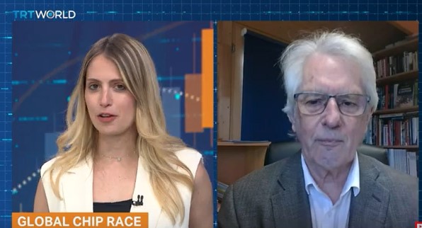
Memory has seen a down-cycle for the last two years. It is now on upside, and recovery will be very strong. It is also the driving force behind the overall recovery we are seeing. The other parts of the semiconductor market, including discretes, have been growing in single digits so far. We are seeing a memory-led recovery. Memory is always the first into the downturn, and first into the upturn.
Regarding the chip war among China, Taiwan, and USA, he added that China is always playing catch-up in terms of technology, which is quite normal. New regions are entering the semiconductor market. It will take time to catch up. China has got two or three nodes in leading edge. China has aspirations for Taiwan. That led the rest of the world to see what can be done to stall China’s entry into Taiwan, and in the high end of the market. That led to the current restrictions on China, led by America. There is this move to push China back, and try to slow it down. They want to keep the lead with TSMC, in particular. The whole world depends on TSMC.
Japan saw modest growth of 4.4 percent last year. How can it maintain growth? Penn noted that Japan was very strong in the 1980s. It was steaming ahead in technology, manufacturing, etc. They have gone from 28 percent share of the global semiconductor market to just 8 percent. They have lost of lot of their OEM segment, which was the market for semiconductors. They have also fallen back in technology.
Japan is now making a very brave effort right now to pull back and catch up. They are certainly doing very well. They have some very good investment projects going on. But, that’s not going to happen overnight. There are huge factors in the equipment industry, huge factors in the materials industry, etc. Japan now has the pieces in place. They need to put their mind to it, and bridge that gap.
Utility-scale quantum computing — advances and future challenges
At IRPS 2024, Dr. Rajeev Malik, Program Director, System Development, Benchmarking & Deployment, IBM Quantum, USA, presented another keynote on utility-scale quantum computing — advances and future challenges. He said quantum timeline started in 1970s with Charles Henry Bennett. It has been advancing since. The field has continued to grow. About five years ago, we introduced Quantum System 1.
Quantum computers are the only novel hardware that changes the game. We need to solve several hard problems. Factoring is involved here. The value of quantum computing becomes apparent as problems scale. They can’t be handled by classical computers. That’s the goal!
We are seeing increasing utility in quantum computing. Any quantum computer can have errors. We are doing error correction, with increasing circuit complexity. We have scale + quality + speed, as performance metrics. These are the three key metrics for delivering quantum computing performance.
Scale involves the number of qubits. Quality is measured as error per layered gate. Quantum computers are noisy, and need to lower the error rates of 2 qubit gates (<0.1 percent). Speed is calcutated in circuit layers per second. We need individual gate operations to complete in <1us range to have reasonable runtimes for real workloads. IBM is striving to bring useful quantum computing to the world, and make it quantum safe.
IBM quantum platform
He talked about IBM quantum platform. We are working on designing the processor, to how users are going to use the system. Qiskit is software development kit, followed by tools that run systems, and users’ work.
A quantum circuit is fundamental unit of quantum computation. A quantum circuit is a computational routine consisting of coherent quantum operations on quantum data, such as qubits, and concurrent real-time classical computation. Relevant problems need 100s and 1000s of qubits and 1 million gates or more to solve.
IBM Quantum Network is mapping interesting problems to quantum circuits. The IBM Quantum Development Roadmap is to run quantum circuits faster on quantum hardware and software. Different things are being used to build qubits. These include photons, ions, solid-state defects, nanowires, neutral atoms, superconducting circuits, etc.
An IBM quantum system has dilution refrigerator with cryogenic interconnects and components, including the processor. It has custom third generation room temperature electronics for control and readout. Classical co-compute servers can enable the qiskit runtime to execute use case workloads efficiently.
IBM quantum roadmap includes demonstrate quantum- centric supercomputing in 2025. We can scale quantim computers by 2027. In 2029, we can deliver fully error-corrected system. In 2030+, we can deliver quantum-centric supercomputers with 1,000s of logical qubits. Beyond 2033, quantum-centric supercomputers will include thousands of qubits capable of running 1 billion gates, unlocking the full power of quantum computing.
From Falcon with 27 qubits in 2019, IBM has moved Osprey with 433 qubits in 2022. We are scaling QPUs, with Osprey using scalable I/O. IBM’s advanced device stackup includes interposer chip, wiring plane, readout plane, and qubit plane. Lot of technologies are borrowed from semiconductors. In 2023, IBM released Condor, pushing the limits of scale and yield with 1,121 qubits. IBM also released Heron with 133 qubits, with I/O complexity on par with Osprey. IBM aims to extend Heron to Flamingo and Crossbill via modular coupling.
Accelerated timescale
We are now upgrading everything, and development is on an accelerated timescale. It is for processors, connectors, control electronics that are getting updated every 12-18 months. Density, power, and cost remain key focus areas. There is migration from discrete to integrated on-board components, and control electronics to 4K temperatures or cryo CMOS. We have longer reliability of cryogenic components. We are looking at predictability, availability, and stability of the system. We have achieved system uptime of over 97 percent, and over 90 percent available to run jobs.
We have deployments in Fraunhofer, Germany, University of Tokyo, Cleveland Clinic, PINQ2 Canada, and pending at Yonsei University, Seoul, Riken, Japan, Iqerbasque, Spain, etc., and 40 innovation centers. We need a disruptive change to unlock potential of quantum computation. We have multiple systems in place by H2-23, with more to come.
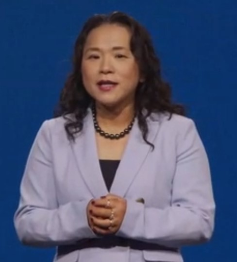
Innovative technologies for sustainable future of semiconductor industry: IRPS 2024
IEEE International Reliability Physics Symposium (IRPS) 2024 was held in Dallas, Texas, USA. Su Jin Ahn, EVP, Advanced Technology Development Office, Samsung Semiconductor R&D Center, presented the plenary on innovative technologies for sustainable future of semiconductor industry.
Semiconductor market growth will be from $224 billion to $350 billion for computing and data storage. Automotive electronics has moved to $150 billion. We are seeing an explosive growth of data and rapid development of AI. Data creation is accelerated by GenAI. We had AlphaGo, developed by London-based DeepMind Technologies, an acquired subsidiary of Google, in 2015.
Today, we are witnessing growth of wafers and semiconductor fabs. Number of fabs using 300mm wafers has increased x3 over last 15 years. There is paradigm shift in computing over the past 80 years. From mainframe era, we have now come hyper-scale connectivity and AI. Moore’s Law-based geometry scaling has been at the heart of all these developments. We have seen evolution of photo-lithograph, multi-patterning, etc. There has been structure and materials innovations as well. There is changing landscape of memory and logic devices in IRPS papers. Reliability issues need to be overcome for new structures and materials.
We are seeing evolution of backend-of-line metals. We have relied on low resistivity and high reliability for performance, speed, and power efficiency of chips. There is evolution of NAND flash memory. It is now entering 3D stack up and WF bonding. Stacking has moved to heterogenous integration. There are mutual thermal, chemical, and stress effects. There are potential reliability issues. Cell-to-cell variations from top to bottom increases due to deep contact hole. There are stress-related problems in wafer bonding.
Technologies in works
We are now in logic scaling trend. CPP scaling has slowed down due to short channel effects, and contact resistance. Cell height scaling slowed down due to rising metal resistance. We have prospects for logic transistor beyond planar TR. We moved from planar TR to FinFeT at 14nm. At 3nm, we have the gate all-around (GAA) MBCFET. At <1nm, we have 3DS FET and CFET.
We have potential reliability issues in GAA transistor. Thin body and process complexity degrade HCI. Structural complexity and increased packing density is vulnerable to heat dissipation. For self-heating, we can maintain temperature at thin nanosheet channels.
We have potential reliability issues in 3DS FET. Accumulation of process damage causes TDDB, and BTI degradation. Complex 3D layout causes Vth variation, and self-heating deteriorates. We also have potential reliability issues in 2D channels. We have to look at material quality, full integration into logic process, defect control, etc.
We have prospects for DRAM cell beyond 10nm. Area scaling continues via vertical channel transistor or vertically-stacked cell array. Potential reliability issues include an undesired hole accumulation in thin floating channel that increases the sub-threshold leakage. Beyond Si-channel, we have deposition-able IGZO channel transistor in vertical channel transistor (VCT). We also have potential reliability issues in IGZO channel. There can be thermal instability in process integration, abnormal PBTI, and ion-Vth trade-off behavior.
Future prospects
In future, we will be transitioning to 3D stack era. We will move to cell array and periphery circuit, and heterogenous integration. We are moving to wafer bonding and advanced packaging. We are seeing the evolution of package technology. We are pursuing fine pitch bonding (<2um) for interconnect density (>2e5/um2) compatible to SoC. We are moving to wafer-to-wafer and multi-chiplets.
There are potential issues in 3D-IC. These include massive bonding interfaces (multi-chiplet, multi-stage HBM) that increases EM risks. Pitch scaling and low temperature process weakens bonding interface stability.
There are several future reliability challenges. They include TDDB, EM, FBE, HCI, BTI, self-heat, etc. Thanks to new semiconductor technologies being developed, we have managed the challenges well, so far. More is expected in future.
Intel launches Gaudi 3 AI accelerator, Lunar Lake, Xeon 6, and more!
Intel Vision 2024 was held recently in Phoenix, Arizona, USA. AI represents a paradigm shift in how humans and technology interact. Pat Gelsinger, Intel CEO talked, about the tangible outcomes AI can enable for businesses, and what the future of AI in enterprise looks like.
He said that we had a proud moment in Arizona on March 20, when we had the first major releases of the CHIPS Act coming to Intel for our Ocotillo facility. It was the largest investment in the semiconductor history. The CHIPS Act is the most important industrial policy since World War 2. Every aspect of our life is becoming digital! Era of AI is driving this huge momentum.
We have Intel Foundry as the systems foundry for the AI era. Intel Products are modular platforms for AI era. Intel Foundry is committed to becoming the world’s no. 2 foundry by the end of the decade. We will also be opening the doors to manufacturing for the first time ever for companies across the industry. Intel Foundry and Intel Products form a deadly combination. We are in the most intense period of innovation.
Every company will be an AI company in the future. AI workload is a key driver of the $1 trillion+ semiconductors TAM by 2030. AI is making everything exciting like we have never seen. It will change every aspect of business.
You need technology infrastructure that is scalable and flexible. You also need tangible business outcomes. Intel has the mission of bringing AI everywhere! We help enable AI for every aspect of your business. Wi-Fi made every office, coffee shop, etc., wireless. AI PC is like the Centrino moment. We are seeing AI PC momentum, using Intel Core Ultra. Over 5 million AI PCs have been shipped to date. We have 40-million-unit goal by end of this year. 500 models are optimized for Core Ultra. We are working with OEM partners like Dell, HP, Lenovo, etc. Our roadmap is strong, and off to a good start.

Welcome Lunar Lake!
Intel’s next platform is the Lunar Lake. It is the second chip we have launched. It is the flagship SoC for next-gen AI PCs. It has 3x the AI performance. It has over 100 platform tops, 45 NPUs tops. The third generation is currently in the fab. We are going to drive the AI PC category.
AI will be creating every new business worker, and automating, streamlining, collaborating, with new insights. You need to refresh! It is the time to upgrade. Today, every app is going through an AI makeover. He encouraged participants to call their IT head and ask for AI PC refresh policy.
The next piece of bringing AI everywhere is the edge and enterprise. The killer app for next-gen edge is AI. Intel is building on the open standards platforms, and investing. There are three laws of the edge — economics, physics, and land. It is too expensive to bring back data to the cloud. Economics says: improve it to the edge. Next, we have skill requirements. Laws of physics drive you to the edge. Laws of the land are also important. Every nation has some form of GDPR capability. Edge is becoming increasingly important.
RAG unleashes data!
We have the retrieval augmented generation (RAG). It’s all about unleashing data! RAG becomes an important workflow for corporations to take advantage of data and GenAI. RAG, as a database and codes domain/business specific data, packages them together for complex queries into open standard LLM environments.
We now have Open Platform for enterprises. How can you deploy using the existing infrastructure, and do seamless integration. Now is the time to build an Open Platform for enterprise AI. We also have strong support from companies listed here, such as SAP, IBM, RedHat, VMware, Yellowbrick, etc. Based on this strong ecosystem, we will have effective benchmarking of these solutions.
Bringing an Open Platform will help with blueprints, reference designs available, and demonstrate performance, interoperability, trustworthiness, and ensure effective benchmarking and certification of these solutions. We will be rolling out next steps for the Open Platform for enterprise AI in Seattle next week.
Lan Guan, Accenture’s Chief AI Officer, said we help customers develop their AI strategies. There are three challenges. One, ambiguous value realization. Clients find hard to realize value from their AI investment. You really need to take the enterprise reinvention approach. The second challenge is the insufficient data quality. GIGO cannot be more truer, especially in the era of AI. As an example, Accenture does so much work in contact center AI. A client had 37 versions of SOP.
Third challenge is the widening talent gap. Many organizations need talents to build, operate, and manage AI. There are also lot of business users that need to be trained for effective prompt engineering.
You need to build with value. It is also time to build your digital core with data and AI foundations. Next, bridge your talent gaps. Further, you need to fix your responsible AI solution. GenAI is also about continued reinvention. Take a marginalized approach.
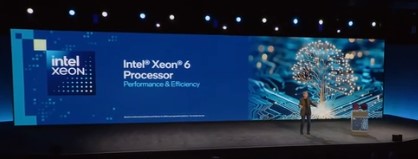
Xeon 6 to the fore
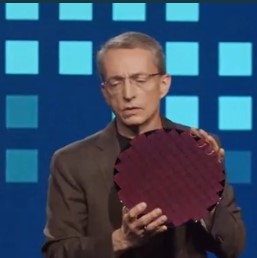
Gelsinger said Intel has been working for years on data center in the cloud. The Xeon innovation machine is not slowing down. We are now seeing rapid evolution of AI workloads. Intel is announcing the next-gen Xeon 6 processors. It is the new brand for next-gen of efficient core and performance core solution.
Xeon 6 with E-core is uniquely addressing the challenges. It is based on Intel 3. We will be moving Sierra Forest into production this quarter, and work with customers and OEMs to make that available. We are delivering 2.7x better rack density. We have 2.5x performance per watt improvements. With Xeon 6, we can reduce the need for telco data centers to just 72 racks, with same performance and capabilities. Xeon 6 provides up to 27 percent lower embodied carbon footprint over previous generation systems.
The big brother of Sierra Forest processor is the Xeon Gen 6 processor, formerly known as Granite Rapids with P-cores. We will be launching this shortly, after the Sierra Forest product. We are excited to be ramping it this year.
We are now looking at maximizing the power of your data. Over 60 percent of data is on the cloud. A vast majority of the data is still on-prem. 66 percent of that data is unused, and 90 percent of unstructured data is unused. LLMs and RAG provide an extraordinary opportunity to unlock this hidden asset. Xeon is tremendous for running RAG environments. It can run LLMs as well.
Intel is working to drive standards, in particular, microscaling formats or MX Alliance. We are working with Arm, Qualcomm, Nvidia, etc. One format is called MXFP4. It is floating 0.4 bit standard for Radix and Mantissa to operate effectively.
Next, we have Xeon 6 P-Core or Granite Rapids. In a Gen 2 vs. Gen 4, test, there is 3X improvement in the latency as we move to modern data types, for FP4. From Gen 4 to Gen 5, there was 100ms threshold. With Gen 6, we have 82ms improvement. We can run hefty models on the Xeon platform. We have 6.4X improvement from Gen 4 to Xeon 6.
Data is now your most valuable asset. Intel is working on confidential computing. We have the EU AI Act, and US Act. We have the Intel TDX. Confidential computing and AI are now available on the cloud with major CSPs. We are building a truly end-to-end confidential computing environment. This is a sweet spot for enterprise AI adoption.
Enterprises are also looking for cost-effective, high-performance enterprise AI training, and inferencing environments as well. They are turning to Intel’s Gaudi 2, which also has price performance advantages. Gaudi is an alternative to Nvidia H100 for training LLMs. We are seeing the acceleration of our Gaudi offering in 2024-25 and beyond.
UEC building AI fabrics
We are now bringing Xeon and Gaudi together. Customers are now asking for open ecosystem for AI connectivity. Ultra Ethernet Consortium (UEC) has the mission to deliver an Ethernet-based open, interoperable, high-performance, full-communications stack architecture to meet the growing network demands of AI and HPC at scale. Intel is among the steering members.
Lhyfe announces progress in green hydrogen projects
Hydrogen producer, Lhyfe, from the city of Nantes, France, started the first production facility into operation in Oct. 2021. Today, the company offers renewable energy solutions, bio-gas, smart grids, and batteries.
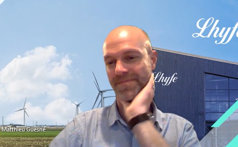
Matthieu Guesné, Chairman and CEO, Lhyfe, talked about their achievements during FY 2023. The FY 2023 revenues were at €1.3 million, which is x2, as compared to FY 2022. Lhyfe had the signature of multiple new clients in France and Germany, including Avia, Manitou, Iveco, John Deer, Hypion, Hype, Symbio, Bretetche Hydrogen, etc.
New sites
Two new sites were inaugurated in France (Buléon and Bessières), making Lhyfe the first producer of renewable hydrogen in the country. Eight other sites are currently in construction or extension, mainly in France and Germany, more than any other player in the sector in Europe. We have continued innovation with the world’s first offshore green hydrogen production.
Lhyfe is also boosting the scale-up, with €149m grant from the French government for 100 MW project near Le Havre in France. It has strengthened financing strategy, with a €28m first green corporate syndicated loan, and increase in secured grants at c230 million, as of December 2023.
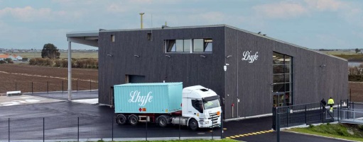
Bouin, France site is now running at full speed. Factory was completed in 2021, and it is now fully booked. Extension is planned for up to 1 ton of green hydrogen/day. This is representing 2.5MW electrolysis installed capacity after extension. The onsite storage capacity will be extended from 700 kg to 5 tonnes. It is scheduled by end of FY 2024.
This is Lhyfe’s first green hydrogen production site with a current production capacity of up to 300 kg of green hydrogen/day (installed capacity of 0.75 MW). It has direct connection to wind farm, and has secured PPA with Vendée Energie. It is serving mobility clients. Lhyfe has 100 percent success rate in deliveries.
Providing site update on Buléon (France), he said it is located in Brittany (Morbihan, Buléon near Lorient). Site has production capacity up to 2 tonnes of green hydrogen per day (5 MW installed capacity). Lhyfe is addressing mobility (70 percent) and bulk industry (30 percent). Main source of energy is wind PPA with VSB énergies Nouvelles. Client has already been signed. Another site was installed as of end 2023. Commercial ramp-up will start by end of H1-2024.
Bessières (France) site update was next. It is located in Occitany (Bessières near Toulouse Occitany). Production capacity is up to 2 tonnes of green hydrogen per day (5 MW installed capacity). Main source of energy is wind PPA. It is also winner of the Corridor Hydrogen tender for projects. This plant is under commissioning. Commercial ramp-up will start by end of H1-2024.
Lhyfe has several sites under construction in Germany. Tübingen, Germany has up to 200 kg per day (1 MW installed capacity). It is aimed at supplying hydrogen-powered trains on the Pforzheim-Horb-Tübingen line from 2024. Lhyfe signed contract with Deusche Bahn. Unit has been installed and ready for client’s start of operations.
Schwäbisch Gmünd, Germany has up to 4 tpd (10 MW installed capacity). It is mostly used for mobility. Construction works was launched at the end 2023. Brake, Germany, has up to 4 tpd (10 MW installed capacity. Site construction had started at end of 2023. It is 100 percent used for bulk.
Sites under construction in France include those in Croixrault and Sorigny. Croixrault has up to 2 tonnes of green hydrogen per day (5 MW of installed electrolysis capacity). It is located on the Mine d’Or industrial area, alongside the A29 motorway. It is the first production unit in the Hauts-de-France region to make renewable hydrogen available to a wide market. It will supply local uses in mobility and industry. Civil works had started early 2024.

Sorigny has up to 2 tonnes of green hydrogen per day (5 MW of installed electrolysis capacity). It is part of Hy’Touraine project. Green hydrogen will be supplied for uses in mobility and industry, with many local authorities and businesses already identified as having hydrogen needs in the area. Civil works started early 2024. In total, Lhyfe will have 10 plants. We are also developing in Spain.
Lhyfe has Fortress pipeline, excluding projects already under construction. Bulk projects are in Wallsend (UK) – 20 MW, HOPE Project (Belgium) – 10 MW, Bussy St-Georges (France) – 5 MW, Vallmoll (Spain) – 15 MW, Duisburg (Germany) – 20 MW, Milan (Italy) – 5 MW, and Le Cheylas (France) – 5 MW.
Onsite projects are in Gonfreville l’Orcher (France) – 100 MW, Nantes Saint-Nazaire Port (France) – 210 MW, Fonderies du Poitou (France) – 100 MW, Epinal (France) – 70 MW, SouthH2Port (Sweden) – 600 MW, Delfzijl (Netherlands) – 200 MW, etc. Backbone projects are in Aaland Island (Finland) – X GW, Lubmin (Germany) – 800 MW, and Perl (Germany) – 70 MW.
Lhyfe has secured €149m grant from French government to support 100 MW project near Le Havre in France. 28,000 m2 available space at the planned site of Gonfreville-l’Orcher. It will produce 100 MW. This confirms Lhyfe’s ability to raise significant subsidies and de-risk large projects. It confirms as well the status as a key player in the renewable hydrogen industry, and know-how and expertise of Lhyfe teams, pioneers in the industry.
The project has been approved by the European Commission as part of the third wave of IPCEI (Important Projects of Common European Interest) on hydrogen.
Offshore hydrogen production
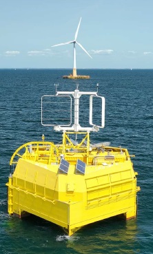
Lhyfe is also paving the way for offshore hydrogen production. SEALHYFE pilot is a unique set of data for a concrete step forward in hydrogen offshore development. It is the first offshore hydrogen production unit in the world in 2022. It is producing green hydrogen offshore in the Atlantic Ocean during pilot period from May-Nov. 2023.
Green hydrogen was produced under stressed conditions (corrosion, direct connexion to wind mill, strong accelerations, fully remote operations). Millions of data was collected to support next phase (HOPE project). Reliability of hydrogen offshore production in an isolated environment, and management of the platform’s movements were undertaken. There was validation of production software and algorithms. It was decommissioned end-Nov. 2023.
HOPE or Hydrogen Offshore Production for Europe, was for the first time in the world. Green hydrogen will be produced at sea, and delivered ashore via
a composite pipeline to local customers for use in industry and transport sectors.
Up to 4 tpd of green hydrogen and 10 MW installed capacity. It is located in the North Sea, off the port of Ostend. Operations are expected early 2026. €33m grants awarded, o/w €20m from EU and €13m from Belgian government. This project is coordinated by Lhyfe, and implemented together with eight European partners.
Aland Island, off west coast of Finland, is an autonomous, demilitarized, Swedish-speaking region of Finland. Lhyfe has project to develop large-scale hydrogen production on Åland, integrated with gigawatt scale offshore wind in Åland waters. It is for use on Åland and in the wider European region. Lhyfe has signed MoU with CIP, the world’s largest dedicated fund manager within the greenfield renewable energy investments, and a global leader in offshore wind, green hydrogen.
Lhyfe is well positioned to answer future offshore bids to be launched in Europe from 2024 onward. Another 80 actions will be implemented over the coming years to address the Group’s ESG strategic orientations. Over 80 tonnes green hydrogen has been produced and sold to date.
