
Metamaterials
Optical metamaterials and metalenses offer novel functions
European Photonics Industry Consortium (EPIC) organized a technology meeting today on metamaterials and metalenses. Corning wafer process solution pairs Corning laser dicing and Dynatex mechanical breaking technology, was a message by the lead sponsor.
Optical metamaterials and metalenses offer many novel functionalities, such as super-resolution imaging, negative optical refraction, beam shaping, and steering. But what is their technology readiness level? In this online meeting, we are going to review the process of industrial adaption of these futuristic technologies in the field and learn from the industry leaders about the first commercially available products comprising metamaterials and metalenses.
Tunable metasurfaces
Junghyun Park, Principal Researcher, Samsung Advanced Institute of Technology (SAIT), South Korea, presented on tunable metasurfaces and its applications. LiDAR has apps in autonomous driving, improving AR/VR, gesture sensing, etc. It can be scanning or non-scanning. Mobile LiDar is present in mobiles, such as flash, spot array, and scanning. Flash has whole area illumination, spot array allows DoE-based spots, etc. Metasurfaces are thin two-dimensional metamaterial layers that allow or inhibit the propagation of electromagnetic waves in desired directions.
When LiDar meets the metasurface, we can get active metasurface. Metamaterials are artificial materials with properties unobtainable in future. Metasurfaces are active vs. passive. We change the control signal for spatio-thermal functions in active. Indium tin oxide is a gate-tunable material. Plasma frequency is tunable. Two control parameters enable complex modulation, Vt and Vb, or top and bottom gates. We can also have solid state beam steering for LiDar apps.
Optical manufacturing
Gauthier Briere, Product Marketing Manager, Applied Materials, presented on optical manufacturing services for metalenses and metaoptics. Its Engineered Optics Group makes optical devices. EO product focus is on waveguides for AR glasses and flat lenses for near IR on 300mm transparent substrate.
Metaoptics is a disruptive technology that you didn’t see coming! Metalenz and STMicroelectronics delivered the world’s first optical metasurface for consumer electronics devices. Metaoptics are available in small-, medium-, and large-size pillars. Metaoptics are in 10s to 10K lens/devices per wafer. Pillar full-wafer CD uniformity control or CDU full wafer 3o- <12nm can be achieved across design-rule CD range.
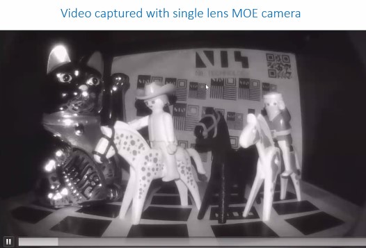
MOE camera
Niklas Hansson, Head of Application Engineering, NIL Technology, presented on NILT’s Single Lens (1 MOE) camera. NIL has meta optical elements (MOEs) and masters for displays (AR/MR). MOEs are for illumination and receiver optics for ToF, LiDar, driver monitoring, and eye tracking. NILT has six class 10-100 cleanrooms.
MOE is a lens technology with potential to disrupt optics used for sensing and imaging. NILT provides custom-made solutions with MOE. Light goes into lens, straight through. We are working on improving efficiency. Single-lens MOE camera eliminates abberation. We have camera with single lens (MOE) surface. We can eliminate field curvature, coma, and astigmatism. Performance is similar to refractive camera. We used pure pillars such as silicon-on-glass, and free form meta-atoms. It uses electron-beam lithography.
Transforming optics and sensing
Rob Devlin, Co-Founder and CEO, Metalenz, presented on meta-optics: transforming sensing and moving optics into semiconductor foundry. Metalenz is transforming optical sensing, and is first fabless semiconductor optics company. It is a spin out from Harvard University, commercializing foundational metasurface IP. It designs and sells meta-optics targeting 3D sensing in consumer electronics and automotive markets.
Metasurface optics manufacturing process enables optics manufacturing in semiconductor foundries. There is a single semiconductor layer used, along with standard semiconductor materials. In 2011, the metasurface came into being. We are sensing disruptions, and enabling proliferation of optical sensing. First Metalenz devices are in the market now. It replaces existing optics in ST FlightSense ToF module.
An example of Gemini was shown, the world’s first dual pattern 3D projector. One projector gives dual patterns. Another example is PolarEyes, that is fit for any form factor. Apps include medical imaging, edge detection, biometric authentication, high-resolution 3D shape reconstruction, etc. Metalenz is enabling supply chain consolidation and proliferation of advanced sensing.
In another sponsor message, PHASICS proposes SID4-sC8 wavefront sensor for the metasurfaces characterization, using quadriwave lateral shearing interferometry or QWLSI technology.
Metalens manufacturing
Patrick Schuster, Process Engineer at EV Group, presented metalens manufacturing using nanoimprint lithography. It has EVG nanoimprint lithography solution for step and repeat or S&R mastering to wafer level imprint. It is an offering to help customers accelerate the deployment of nanoimprint lithography (NIL) in high-volume manufacturing. SmartNIL enables replication of different geometries/orientation and dimensions.
We can design to imprint and provide pattern fidelity. NIL at EVG does wafer-level based manufacturing, provides SmartNIL technology and open materials platform. NILPhotonics Competence Center is an innovation incubator. It is currently looking for a mastering partner, along with new materials. EVG-Toppan has a whitepaper on manufacturing of metalenses using NIL.
Challenges and opportunities
Lieven Penninck, Founder, PlanOpSim, presented a view on opportunities and challenges for design of metalenses and metasurfaces. There are bottlenecks in metasurface design. We need integration to system level, have fast large-area design, and design for manufacture is in an embryonic stage.
For system integration, we have to optimize using ray tracing system design for idealized metasurface. We also have metasurfaces informed system design, and cascaded to co-optimized design. Time consuming aspect of design is simulation of nanostructures. We need to reduce loop time. For high-speed large area design, we have inverse design, and surrogate solver. We have combined optimization and network. We need large training set. Future work includes wide applicability and larger area. Component tolerancing should be linked to system tolerance. We have Monte Carlo study for tolerance analysis. Monte-Carlo simulation is the most popular and simplest method for nonlinear statistical tolerance analysis.
Ms. Maryvonne Chalony, Application Engineering Manager, Synopsys, presented the MetaOptic Designer, a fully automated commercial tool for metasurfaces optimization. The existing metalens design approach is semi-automatic, multi-domain approach.
Synopsys released in Sept. 2022, MetaOptic Designer, a fully automated tool with inverse design capability. It automatically generates metalens/metasurface layouts, RSoft CAD files for simulation, and GDS lines for fabrication. It reduces the level of knowledge and expertise required, shortens design cycle, and saves money and space. MetaOptic Designer determines the design parameters across each metasurface, and exports GDS and optimization results. We can also combine refractive lenses and metalenses.
